
I have been keeping a blog as I have worked through testing the HDL generated from the captured ALD diagrams. Here are the entries:
- The FPGA Simulated IBM 1410 has a “pulse”
- IBM 1410 FPGA Simulation – The Brainstem
- IBM SMS Generation Application
- Instructional Logic Diagrams and Automated Logic Diagrams
- IBM 1410 ALD Volume II Completed
- The first missing IBM 1410 ALD Sheet
- A couple of errors in the IBM 1410 System Fundamentals manual
- Q: When is a Capacitor not “just a capacitor”
- IBM 1410 ALD / FPGA Progress Report: Volume III Complete
- IBM 1410 ALD to FPGA – I “got one”
- IBM 1410 ALD to FPGA – Punch Column Binary ALD anomaly
- IBM 1410 FPGA – A Tale of Two Sheets
- IBM 1410 ALD to FPGA Another one bites the dust!
- IBM 1410 ALD to FPGA: Volume V complete – a “quickie”
- 1410 ALD to FPGA Volume VI is in the bag
- IBM 1410 ALD to FPGA: Volume VII Testing Now Complete
- IBM 1410 ALD to FPGA Volume VIII complete – only two to go
- Volume IX is Now a Memory
- 1410 FPGA – ALD Generation Test Completed
- IBM 1410 FPGA – Simulation and Initial FPGA Programming
- IBM 1410 FPGA – FPGA Testing and Memory
- IBM 1410 FPGA: Console Output
- IBM 1410 PFGA: Posted to Github
- IBM 1410 FPGA: Serial Output FIFO and Arbitration
- IBM 1410 FPGA: Inputs
- IBM1410 FPGA: More Inputs
- IBM 1410 FPGA Core Memory Upload — Dual Ported CORE??
- IBM 1410 FPGA: Diagnostics!!!
- IBM 1410 FPGA: Off to the Races??
- IBM 1410 FPGA: “Space Cadet”
- IBM 1410 FPGA: 1401 Mode “Zoned Out”
- IBM 1410 FPGA: (Address) Exit Stage Right
- IBM 1410 FPGA: 1401 Mode SAR Instruction
- IBM 1410 FPGA: S’more SAR Instruction Issues
- IBM 1410 FPGA: We ain’t got no 1401 Overflow anymore?
- IBM 1410 FPGA: No. 5 sez: Need More Input
- IBM 1410 FPGA: Input Check
- IBM 1410 FPGA: TAU Not So Fast
- IBM 1410 FPGA: From USB Serial to UDP over Ethernet
- IBM 1410 FPGA: Wrong Wrong Length Record
- IBM 1410 FPGA: Overlapped I/O Fix
My current project, underway for more than three years, is to capture the information from the IBM 1410 hardware drawings in a database in order to generate HDL to implement the 1411 CPU in a Field Programmable Gate Array (FPGA).
Most of the materials used for this effort can be found on the Computer History Museum’s bitsavers.org website.
The first thing one must do in such an effort was to design a database to capture the information.
The next step was to analyze the individual Standard Modular System (SMS) card circuits in order to eventually create equivalent logic equations or HDL.
As of February, 2020, the application source (GPL) and the database itself are available on github at https://github.com/cube1us/IBM1410SMS .
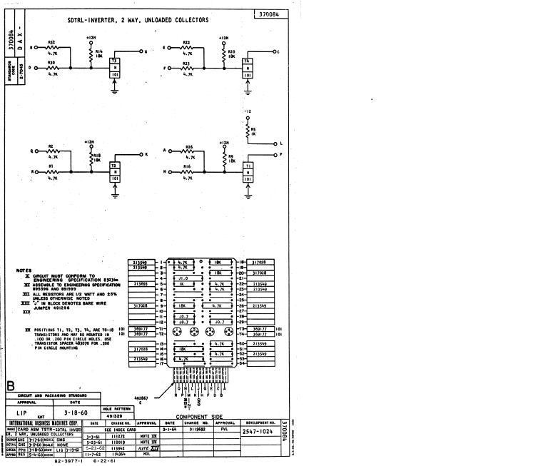
Here is a sample page of such a circuit card diagram (for a better look follow the bitsavers.org link above.)
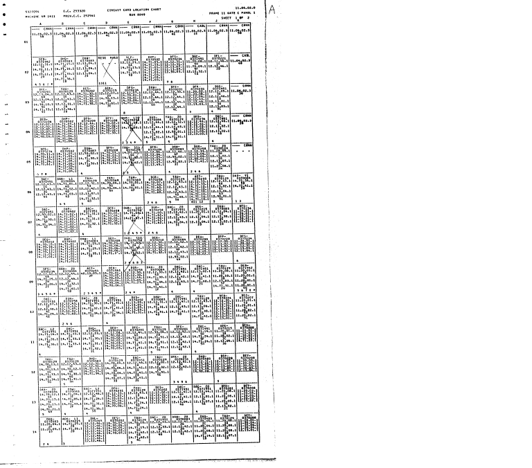
The next phase was to capture what card type was located in each card slot, along with usually identifying all or a substantial number of logic blocks, or gates, on each Automated Logic Diagram (ALD) page. To do that I entered the information found on the ALD Card Location charts, a sample of which is shown below, into spreadsheets. There were four frames, comprising about 14 panels, each panel taking up two sheets like that shown here. I then imported those spreadsheets with part of my application to enter the data into the database.
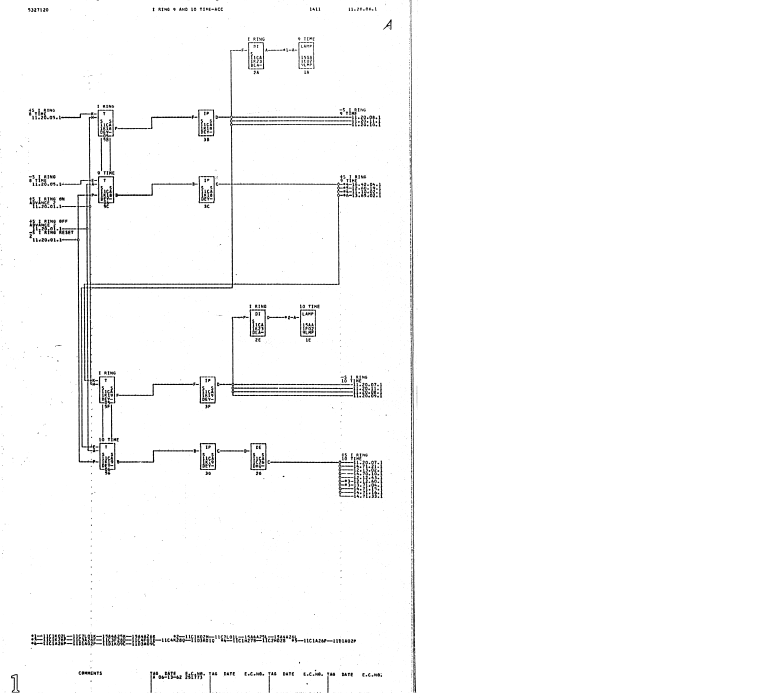
Once that was done, the next step was to process the actual ALD diagram sheets, which comprised 10,596 individual logic blocks, 14,021 signals coming on and off the sheets with 4,222 individual distinct signal names, and a whopping 32,746 connections between logic blocks, “dotted” (wired and) connections and those sheet edge signals. Below is one of the simpler ALD diagram pages.
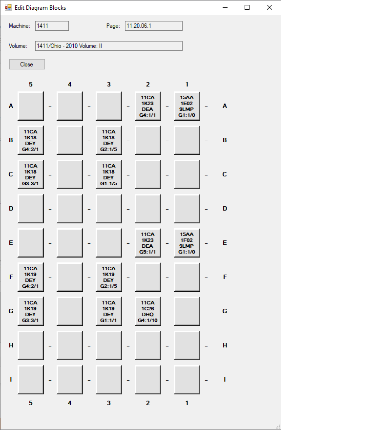
Here is a screenshot of the application showing this same page. Clicking on a given logic block in the application allows entering/editing detailed information about that logic block and access to another sub-page for entering/editing connections.
Update: 6/14/2020 Much has happened over the past few months. The SMS data application now successfully generates most ordinary ALD pages, including those with triggers (defined flip flops) and “latches” (cross connected gates). It also now supports recognition of bussed inputs and outputs when a group of related pages are specified during HDL Group generation (but not for individual pages.)
I have successfully sythesized the main oscillator and logic clocks, and the I ring used for instruction readout. The logic clocks were also tested on a real FPGA development board.
Update: As of November 4, 2020, I have completed test generation of each and every ALD page, and tested them with test benches – fixing bugs, errors in the data, etc., along the way. The FPGA implementation, in VHDL, is available on github at https://github.com/cube1us/IBM1410FPGA
Update: As of June 11, 2022, the CPU seems to mostly run correctly, and a console support application has been developed, and is now available on github as well. https://github.com/cube1us/IBM1410Console
Update: As of July, 2023 the FPGA now passes at least one major 1410 diagnostic, and I am beginning to work on checking out 1401 mode, which is now mostly working.
Update: As of early August, 2023, the FPGA now passes both the 1410 Diagnostic CU01 and the 1410 1401 mode diagnostic M011A.