Having fixed the 1401 Store B Register instruction and gotten further in the 1410 1401 mode diagnostic program M011, it was time to look at the Store A Address Register (SAR) instruction again.
The CE Instruction materials say:
“Therefore the A address left from the previous operation must move to the BAR before the new A address reads in. This is done during a B cycle that occurs just after the Q-op is detected at I-op time.”
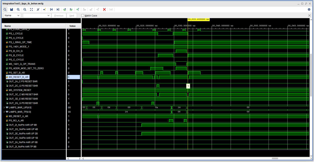
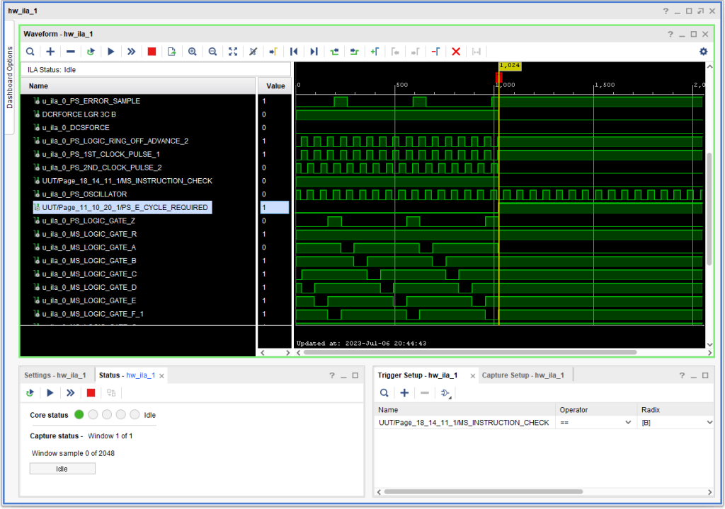
The first timing diagram, below shows that the +S RO A AR signal that presumably ought to be making the AAR contents available becomes inactive before the BAR is reset, so the BAR never receives valid contents – it ends up with invalid binary zeros. (In the 1410, the address registers contain 2 out of 5 code – and having no bits set at all is invalid.) The result was a number of errors, halting the CPU, as would be expected – B Channel, Address Channel, and B Character Select (because the resulting memory address was invalid, none of the 10K “core” modules was selected.
Timing diagram showing issue reading out A Address when setting B Address
There is a signal which looks like maybe it was intended to force the readout of the A Address Register – -S 1401 Q OP TRANS, however once the B cycle starts, the B Character register was cleared and so the signals that relied on – the “Q” character with at wordmark were no there once the B data register was reset early in the B Cycle.
This does not seem to be a race condition. Rather, I suspect it is resulting from the fact that some of the pages for the signals involved are for a 1410 with the accelerator feature, and some without. My hunch is that on a 1410 with the accelerator feature, all of the needed activities to copy the AAR to the BAR occur during the I OP cycle, driven by the -S 1401 Q OP TRANS signal. However, when I tried to force it that way, I was not successful.
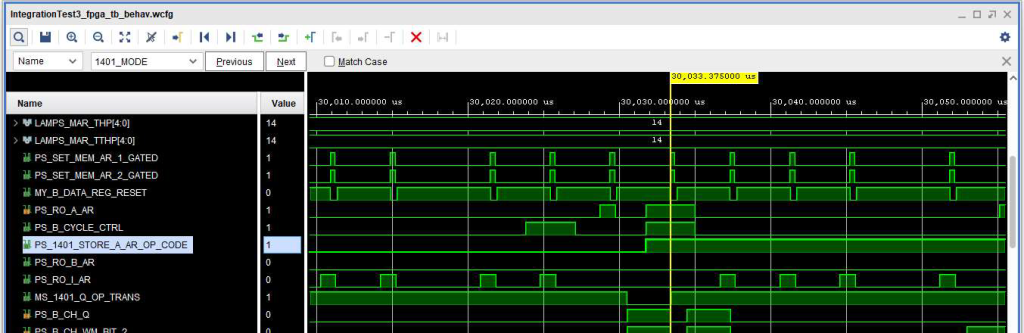
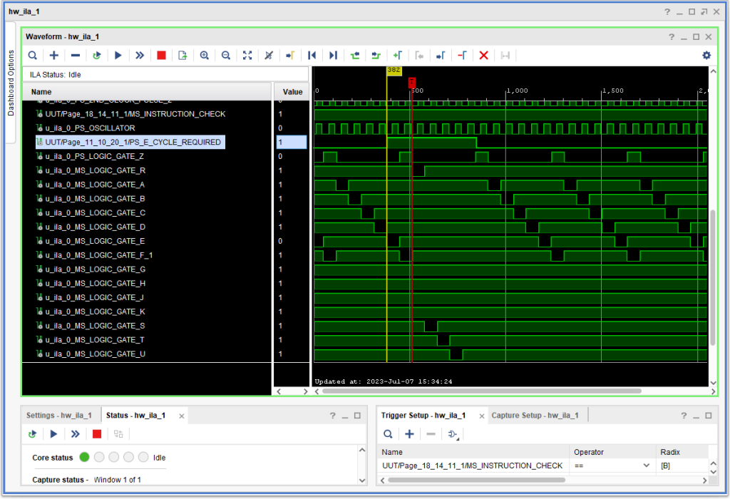
To work around the problem, I added logic to ALD page 14.71.30.1 (A Address Register Readout) to read out the AAR when signals +S 1401 MODE 1 AND +S STORE A AR OP CODE AND +S B CYCLE CONTROL are all active. The result was the timing diagram below (sorry that it is only half of the signals, but the important ones are there.) With that change, the +S RO AAR is active through the necessary part of the B Cycle so that the contents of the AAR are properly transferred to the BAR.
Timing diagram showing fix to page 14.71.30.1 to read out AAR when setting BAR during B Cycle.
With that fix in place, the diagnostics mostly run but fail with console error message “ERR 601J”. So, on to the next fix…
With the 1410 mode CPU running correctly, it was time to test out the 1401 side of things. The 1410 has a toggle switch, allowing the CPU to run as an IBM 1401 compatible with most 1401 programs. The 1410 and 1401 are similar, architecturally. The biggest difference is that the 1401 uses 3 character addresses, with the zone bits over the units and hundreds positions in order to address up to 16,000 characters, whereas the 1410 uses 4 character addresses, capable of addressing memory up to 100,000 characters.
The primary 1401 diagnostic is M011. Once I figured out a problem involving the 1401 addressing scheme, I turned my attention to the next failure: The Store A Address Register (SAR) instruction died a horrible death with B Channel, Address Channel and B Character Select Errors. That problem manifested as a failure to copy the A Address Register to the B Address Register for storing later. I tried for a bit to fix this first, but was not immediately successful, so I decided to try and NOP out the uses of SAR, that mostly had to do with storing the address of each test so it could print out a failure message.
Having done so, the next problem quickly cropped up: the partner instruction for the B address register, Store B Address Register (SBR) also failed – it is essentially the same as SAR, but without that first step of transferring the AAR to the BAR. And the failure error was different as well: an Address Chanel Exit error. The ALD for this circuit is 18.14.02.1 . The ILD is on figure 59 at coordinate 2B – however there is also an error in that ILD. It shows the GateOff input to trigger DEZ as ground (the usual ground symbol). However, on the ALD, the F input it connect to M, which is -12 Volts, and in my scheme, that is logic 0. (Logic 1 being 0V).
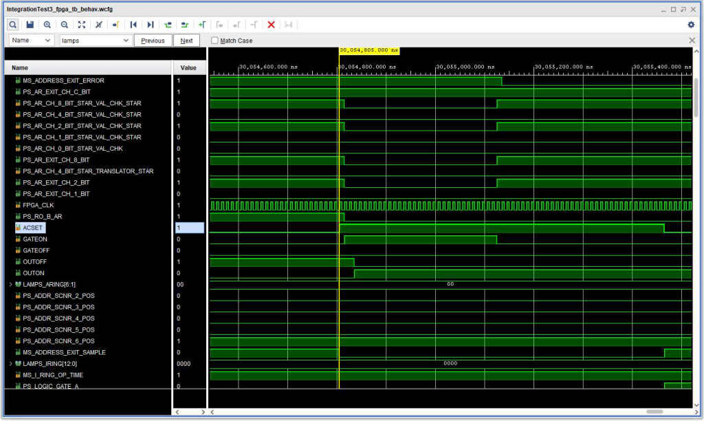
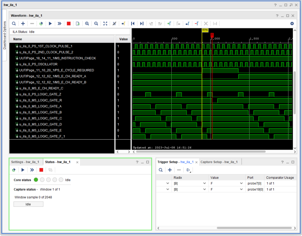
The timing diagram below shows the timing issue. The B Address Register read out and validity check look like they are OK with respect to the Address Exit flip flop ACSET signal. However, the problem was that the VHDL for implementing the SMS card type DEZ has a 3 clock cycle “silo” for ACSET, so that the flip flop is not really set until 3 clock cycles after its ACSET input. In addition, there was no such silo for the other inputs. This silo was put in place to give the ACSET signal some noise immunity – so that a 1 cycle glitch would not set the trigger. But the fact that the other inputs did not have a silo meant that they were sampled 3 clock cycles (FPGA_CLK) after ACSET, and by that time the B Address Register Readout signal (PS_RO_B_AR, i.e. +S RO B AR) had become inactive.
Delay in the Address Exit Check inputs with respect to the readout of the B address Register, resulting in an Address Exit Check.
The relevant VHDL looked like this:
   SMS_DEZ_PROCESS: process(FPGA_CLK, ACSET, DCSET, DCRESET, DCRFORCE, DCSFORCE)
        begin
        if(rising_edge(FPGA_CLK)) then
           if(DCRESET = '0' OR DCRFORCE = '1') then
              OUTOFF <= '1';
              OUTON <= '0';
              SSTAGE1 <= ACSET;
              SSTAGE2 <= ACSET;
              SSTAGE3 <= ACSET;
           elsif(DCSET = '0' OR DCSFORCE = '1') then
              OUTON <= '1';
              OUTOFF <= '0';
              SSTAGE1 <= ACSET;
              SSTAGE2 <= ACSET;
              SSTAGE3 <= ACSET;
           else
              SSTAGE1 <= ACSET;
              SSTAGE2 <= SSTAGE1;
              SSTAGE3 <= SSTAGE2;
              if(GATEON = '1' AND SSTAGE2 = '1' AND
                SSTAGE1 = '1' AND SSTAGE3 = '0') then
                  OUTON <= '1';
                  OUTOFF <= '0';
                elsif(GATEOFF = '1' AND SSTAGE2 = '1' AND
                  SSTAGE1 = '1' AND SSTAGE3 = '0') then
                   OUTOFF <= '1';
                   OUTON <= '0';
               end if;
            end if;
        end if;
        end process;
Once I realized what was going on, the fix was pretty easy. Just add a 3 clock silo for the inputs as well as ACSET. I took the conservative approach, however, and created a separate special instance of SMS_DEZ.vhdl, called SMS_DEZ_SYNC.vhdl to use in the Address Exit validity check logic. This new implementation of DEZ would probably work fine across the board, but I am just using it in the one place, for now.
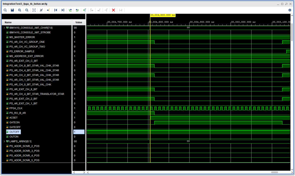
The timing diagram below shows that now the OUTON signal does not activate – no Address Exit Check, because now the inputs are sampled at the same time as ACSET, and those inputs are still active from the B Address Register readout.
Timing diagram for 1401 mode SBR after fixes.
The relevant VHDL looks like this, for gate type SMS_DEZ_SYNC:
    SMS_DEZ_PROCESS: process(FPGA_CLK, ACSET, DCSET, DCRESET, DCRFORCE, DCSFORCE)
        begin
        if(rising_edge(FPGA_CLK)) then
           if(DCRESET = '0' OR DCRFORCE = '1') then
              OUTOFF <= '1';
              OUTON <= '0';
              SSTAGE1 <= ACSET;
              SSTAGE2 <= ACSET;
              SSTAGE3 <= ACSET;
              GON1 <= GATEON;
              GON2 <= GATEON;
              GON3 <= GATEON;
              GOFF1 <= GATEOFF;
              GOFF2 <= GATEOFF;
              GOFF3 <= GATEOFF;
           elsif(DCSET = '0' OR DCSFORCE = '1') then
              OUTON <= '1';
              OUTOFF <= '0';
              SSTAGE1 <= ACSET;
              SSTAGE2 <= ACSET;
              SSTAGE3 <= ACSET;
              GON1 <= GATEON;
              GON2 <= GATEON;
              GON3 <= GATEON;
              GOFF1 <= GATEOFF;
              GOFF2 <= GATEOFF;
              GOFF3 <= GATEOFF;
           else
              SSTAGE1 <= ACSET;
              SSTAGE2 <= SSTAGE1;
              SSTAGE3 <= SSTAGE2;
              GON1 <= GATEON;
              GON2 <= GON1;
              GON3 <= GON2;
              GOFF1 <= GATEOFF;
              GOFF2 <= GOFF1;
              GOFF3 <= GOFF2;
              if(GON3 = '1' AND GON2 = '1' AND GON1 = '1' AND GATEON = '1' AND
                SSTAGE2 = '1' AND  SSTAGE1 = '1' AND SSTAGE3 = '0') then
                  OUTON <= '1';
                  OUTOFF <= '0';
                elsif(GOFF3 = '1' AND GOFF2 = '1' AND GOFF1 = '1' and GATEOFF = '1' AND
                  SSTAGE2 = '1' AND SSTAGE1 = '1' AND SSTAGE3 = '0') then
                   OUTOFF <= '1';
                   OUTON <= '0';
               end if;
            end if;
        end if;
        end process;
With that out of the way, I could run M011 diagnostics quite far into the tests, until it needed to use the SAR instruction for more than just tracking the test address.
Having fixed the problem with the space, I continued to test out the IBM 1410 in 1401 mode. At first, I had thought that it was getting quite far in the diagnostic M011 – it would error out with the I register (instruction counter) at 6029. I spent the better part of a day chasing down an apparent problem with the Store A Address Register (SAR – opcode Q) instruction at the indicate location. However, when I placed a halt at the test before that, it still failed at the same place. How could that be?
So, I decided it would be worth the trouble to run the 1401 diagnostic in Instruction Fetch/Execute mode (I/E). The problem became apparent much more quickly than I had anticipated. After halting at the halt and branch instruction at location 2018, it ended up trying to fetch an instruction at a location near 06020. (My memory is just a little fuzzy on when that flying leap actually occurred, and I don’t have the output anymore.)
As you may know, the 1410 has 5 digit addresses, whereas the 1401 used 3 digit addresses plus zone bits to address up to 16K of memory. It was clear that somehow the translation from the 1401 style address to the 1410 address register had gone awry.
A little digging reminded me that there was one page of the automated logic diagrams (ALDs) associated with this translation, part of what is called the “Zone Adder” that was missing – page 14.18.04.1. After some time working with the xsim simulator under Vivado, I began to suspect a problem with my re-creation of the logic from that page.
Input “A”: -S ZONE ADDER A A DOT B A
Input “B”: +S ZONE ADDER B BITS EVEN
Output “O”: +S A NOT A DOT B A DOT B BITS EVEN
The output name is sufficiently complicated that the equation for this is not self-evident. Looking at the ILD figure 55, it looks like the following should be the equation:
O <= NOT A and NOT B — The NOT A is because A, above is -S not +S
Interestingly, page 14.18.04.1 is not referenced at all in the 1410 1401 Compatibility manual on page 7. On both the ILD and that manual, this signal is routed to the middle of a logical OR gate labeled “Zone Adder Carry”, which is laid out on page 14.18.06.1.
Regardless this VHDL caused the problem noted above. However, I had also penciled in on the ILD an additional inverter, which would be the signal without the added inverter (double negative and all that…). For that, the equation would be:
O <= NOT(NOT A and NOT B)
And it actually takes one less “fudged” gate, because the SDRTL provides this result outright.
It turns out that removing that inverter from the logic for that ALD (and thus implementing this second equation) cured that particular problem, both under xsim and running on the FPGA. But, at least superficially, this makes it look like it does not match the ILD — at least at first.
However, and finally, examining the page to which this signal is routed, 14.18.06.1, one sees that it is routed to a logical OR (physical NAND) gate where -S / -B active inputs generated the +S active output. So if one takes the two together, the end result is such that it does match the ILD.
The diagnostic didn’t get very much further, however, and now fails at location 2032 on a SAR instruction, similar to the failure after the “flying leap” problem, just at a different location. SAR is interesting in that it first copies the A Address Register to the B Address Register, and that is apparently failing.
No, not that kind of cadet. Unlike the IBM 1620, the IBM 1410 does have adder circuits for doing addition (and multiplication and division as well). Instead, this issue had to do with the IBM 1415 space function.
I had thought that the principle instruction diagnostic, CU01, was working perfectly, but it was not quite so. I had noticed that even after finishing the diagnostic, I kept getting space characters sent to the PC support program, but figured that was just a software bug somewhere. However, when I started to run IBM 1410 1401 compatibility diagnostic M011, it stopped typing its instructional message to switch to 1401 mode on the console when it hit the first space character.
After some sleuthing, I discovered that the console typewriter logic never asked the channel for the character after the space – it just kept sending that space to the console typewriter again and again and again.
As one might expect, the issue turned out to be in the console typewriter Selectric emulation VHDL code. I had miss-interpreted the signal -V CON PRINTER SPACE NO to just involve console input via the space bar. a closer look at the related automated logic diagrams (ALDs) made me realize that in fact this was also the Selectric’s way of telling the 1411 that the space process had been completed, and that it really had nothing to do with input from the space bar.
At first I tried to just use the relevant states of the finite state machine (FSM) that controls spacing. That did not work right, however, because that same FSM also controls back-spacing. Qualifying the logic signal to only be active during a space, but not backspace, operation filled the bill.
Once the 1415 console emulation was up and running, I was able to run diagnostics. The first set of diagnostic failures arose in the Assembly Channel because the Automated Logic Diagrams I had for parts of the Assembly Channel were not for the 1410 Accelerator feature, unlike the vast majority of ALD pages I had.
Once I fixed that, diagnostic CU01 ran OK in non-overlapped non-priority (interrupt) mode. However, once I enabled overlapped I/O with the priority feature in the diagnostic settings, the diagnostic errored out with an Instruction Check. The overlapped I/O is that of the 1415 console. The diagnostic then monitors that (along with a priority interrupt) to make sure that the channel status information and the interrupt operate as expected.
The Assembly Channel issue had been reproducible using a single instruction, and I could set that instruction in the initialization of the first 10K memory module, so I was able to troubleshoot it using simulation. But not this one – it happens after 10s of thousands of instructions. I had been less than confident about using the built-in logic analyzer capability that Vivado affords for Xilinx chips, but this problem left me no choice. Fortunately, after just one false start, I was able to figure out how to make a change in the signals the logic analyzer had available, set triggers, and so on – so, not so bad.
Here is what the problem looked like that caused the Instruction Check. Note that the signal +S E CYCLE REQUIRED is going active (high) just after signal -S LOGIC GATE A. Now, that should not be a problem, except that +S ERROR SAMPLE is also high at this point, and since Logic Gate A is active, as well as E Cycle Required, the logic in the CPU sees that as a possible problem – knowing that if E Cycle Required is active, it ought to be activating Logic Gate R rather than Logic Gate A. (Note: At this point I had not included +S E CYCLE REQUIRED A (one of four different ways that +S E CYCLE REQUIRED can be asserted – and which turned out to be the “villan” in this case. Anyway, here is what the output of the logic analyzer looked like:
E Cycle Required Request with a Race Condition
Now, this was not occurring on all or even anywhere near a majority of overlapped I/O operations. Below is an example (using the very same FPGA configuration) of a successful overlap. Note that in this example, +S E CYCLE REQUIRED is asserted much earlier – along with -S LOGIC GATE E so there is no race – E Cycle Required is ready and present long before the time of+S LOGIC GATE Z when the CPU makes the decision between Logic Gate A and Logic Gate R is made.
IBM 1410 FPGA Overlapped I/O Cycle With No Race Condition
So, I went looking for possibilities:
Had I made a mistake when I entered the data for the associated ALDs?
Was this a race condition caused by the fact that I insert “D” flip flops to disconnect any timing loop identified by my generation code (within a single ALD) or by Vivado during synthesis (involving multiple ALDs)?
Was this a race condition caused because the FPGA gates are much faster than the original RTL logic SMS cards, and/or the fact that LUTs are used to collapse combinatorial logic into a decision table that may eliminate multiple levels of original gates?
Was this a very tight timing window in the original CPU?
During my investigation I came upon this tidbit in manual 226-2692, IBM Customer Engineering Instruction-Reference 1411 Input-Output Operations on page 46:
Service Note Because close timing conditions occur in the areas listed below, excessive delay, or accumulated delays in the logic circuits may cause machine failures: CHANNEL REGISTERS AND CONTROLS E-cycle required F-cycle required E-cycle control F-cycle control Address channel
Well, do any of those look familiar? Like maybe the italicized one? While I have resolved the issue, I do not know, for sure, the exact nature of why I ran into it. The original CPU had the +S E CYCLE REQUIRED signal originating in (physical) Frame “D”, whereas the logic gate signals are created in Frame “C”, a couple of feet apart. As a guess I think it is most likely the the FPGA logic is faster than the original hardware in this area, such that +S E CYCLE REQUIRED could be being asserted earlier than the original engineers thought probable.
Regardless, I faced the issue of what to do about it. I had several choices:
I could try and tweak my generated logic in terms of speed, by adding delays, to see if I could resolve it that way.
I could inhibit +S E CYCLE REQUIRED A (the one that seemed problematic) in the presence of -S LOGIC GATE A so that in such a case, the E Cycle Required signal would not be asserted until near the end of the memory cycle of this enar miss.
I could inhibit +S E CYCLE REQUIRED (so, all four possibilities) in the presence of -S LOGIC GATE A
The first two choices might work, but would leave me in a situation where this problem could recur later on, in some other setting, whereas the third option would prevent it from happening a priori. The only downside that I could see would be that it might prevent a device from transferring data to memory quite as fast as the original.
So I investigated transfer speeds of various devices to see what they might be like:
Unit record devices have a core buffer in the IBM 1414 I/O Synchronizer, and are slow enough anyway, that it would not likely make any observable difference.
IBM 729 tape drives. The 729 IV transfers at 112.5 IPS at 556 CPI, the 729 VI at 112.6 IPS at 800 CPI. So, roughly, 112.6*800 = 90,080 cps, or a bit over 11 micro-seconds per character. So, every other cycle would be fine on a an 1410 with the Accelerator feature with 4.0 microsecond cycles – allowing it to “steal” every other core cycle.
IBM 7340 Hypertape Drives. Some models are 112.5 IPS / 170,000 cps tape drives (so, roughly 1500 CPI), or 5.9 microseconds/character. That would require making transfers in non-overlapped mode (see the 1302 disk drive, below). However, ones attached to a 1410 more likely operated at 34,000 cps – plenty slow enough.
A 1405 Disk Drive spins at 1200 RPM (so only 20 rps) and has a 1000 character track size (so, say 1200 to be conservative). That gives us about (1/20)/1200, or 50ms/1200, or 41 microseconds per character – lots of time.
A 1301 transfers characters at 90,100 cps, or 11 microseconds per character – so plenty of time using every other core storage cycle.
A 1302 transfers characters at 184,000 cps, or 5.4 microseconds per character. But on a 1410, these devices transfer data only in non-overlapped mode (even if the I/O instruction specifies overlapped mode) – because they must use consecutive storage cycles for their data.
A 1311 (the 2311 is not supported) has 2980 characters/track, and rotates at 40ms/revolution. this gives us roughly 13 microseconds per character.
These point to things being OK so long as the peripheral can “steal” every other core cycle. On top of that, the 1410 Channels are double buffered, so even if sometimes it takes 5 cycles to get two characters in or out, operation should not be affected. It would not seem the peripheral speed would prevent using the last option listed.
So, I made the changes, labeling them with a fictitious ECO “JRJ001” in the database and tested – diagnostic CU01 now passes without problems. Below is what the signals look like, timing wise. I believe (but cannot prove) that what happened is that +S E CYCLE REQUIRED ended up delaying until the next possible “last logic gate” (in a given memory cycle), which is typically logic gate E, as is the case in this capture.
E Cycle Required after Installing “ECO” JRJ001
So, what is next on the block?
Several enhancements to the console program, including merging what is now the main root window with the 1415 console form – no need to have them separate.
Run more diagnostics, by saving core images under my software simulator and transferring them to the FPGA memory to read them, as I did with CU01.
Experiments with speeds: how fast can I run the 1411 CPU before it fails its diagnostics?
Research into channel signals. I don’t have ALDs for the relevant IBM 1414 I/O Synchronizers, though I do have ILDs, which pretty well define the logic. But rather than parroting exactly what the 1414s would have done, I will likely just use VHDL using some of that ILD logic as a wrapper around communication to and from the PC support program, at least at first.
With the console typewriter working, and the ability to load core images, I was now ready to try and run some diagnostics. The first issue I ran into was that the main diagnostics, CU01, was initialized for 80K of core. That the core image file was larger wasn’t an issue: the Windows based support program knows to only send the first 40K. However, there was a flag denoting machine size that needed to be “patched” — which I did using my emulator, and then saved as a new core image.
Loading the diagnostic, it typed out its identifier, but then quickly errored out with an Assembly Channel error on a Subtract instruction where the destination B-field was initially positive, but turned negative during the subtraction. This was not the first place I expected to see an issue – figured it would more likely relate to some trigger or other. But nope, this was a simple issue in the Assembly Channel.
The problem arose because the ALD diagrams I have are mostly for an IBM 1410 with the Accelerator special feature, however, most of the ALD diagrams for the Assembly channel proper (ALD 15.50.xx.1) are for the non-accelerated version whereas the Assembly channel controls (ALD 15.49.xx.1) are for the accelerated version. There were several signals that ended up either not being used, or having no source as a result:
-B B CH MIN+INV PLUS SIGN GATED
-B B CH PLU+IN MIN SIGN GATED
-B B MN +IN PL+PL+INV MN GATED
These all relate to cases where the B field ends up with a sign other than its original sign. I suspect that the idea was that these signals provided earlier gating to the assembly channel rather than just deriving them from the adder with additional gate delays.
After fixing the Subtract issues which involved just the “B” bit on page 15.50.06.1, (going from positive to negative) I immediately ran into the same issue on the first pass of the diagnostic during the same test, changing from negative to a positive result. Fixing this involved pages 15.50.05.1 (mostly). As a result the pages for the Assembly channel have some gates who’s note at the top is “FUDGED”. 😉
With that, so long as I didn’t enable I/O overlap and Priority Alert (interrupts) during the test, CU01 completed successfully! Frankly this was something of a surprise: It tests most of the instructions and ways of moving data and they all just worked.
Also, the run time of about 3.75 minutes matches very well with the information in the diagnostic listing for a 1410 with the Accelerated logic feature.
So then, I ran it again, but with overlapped I/O and priority features turned on in the diagnostic. It ran fine for about a minute, but then failed during overlapped execution of a multiply instruction. More on this during the next installment.