I learned today that Professor Marleau passed away in 2021. I took a couple of courses from him. If I remember correctly, the first was ECE 331 State Space Systems Analysis. It was hard. Then, the next summer, in 1972, I did an independent study course with him working on very rudimentary computer graphics software. (Mostly, it was so slow that it made a really good case for the need for a separate graphics processor, the VT11 and the GT40 system.)
Many years later, while I and Hannes Beinert were acquiring computers for my collection, I learned through UW Surplus that Professor Marleau was decommissioning a large amount of DEC PDP-11 minicomputer equipment to make way for a new generation of equipment based on Unix workstations. He graciously arranged, through UW Surplus, for the entire set of equipment, manuals, tapes and disks to come into my possession, where the equipment still remains. Recently, I started the process of scanning in the documentation, and making it available on my Google drive and hopefully, should they see fit, on the bitsavers.org website.
More information on Professor Marleau can be found at the ECE Emeritus page in his honor (which also includes a link to his obituary.)
Overlapped Tape I/O is generally working OK now. Getting that to work involved two things.
Firstly, I needed a delay corresponding to the tape inter-record gap time (though not nearly that long) so that the several instructions that the diagnostic runs through before it tests for an overlapped condition would occur while an I/O Overlap still in progress. This fixed the error stop problem. Fortunately, that was much easier to find and fix than I had expected.
After fixing that problem, overlapped reads worked correctly, but overlapped writes had a problem – they somtimes dddduplicated characters 😉 – resulting in records longer than they should have been (and with incorrect contents).
The latter turned out to be more or less self inflicted. In August of 2023, I encountered some issues with the Store A Address Register (SAR) instruction. To fix that I used the +S ADDR MOD SET TO ZERO signal to inhibit resetting the modify by zero address modifier control latch, reasoning that latches don’t respond well to having simultaneous set and reset signals active at the same time.
In this case, however, that was causing the Modify by Zero Address Latch to not reset at times when it needed to, which then sometimes inhibited the Modify by +1 Address Latch from setting, causing the address for the I/O to not increment properly.
The fix was to modify the ALD that generates the address modificatio signals, ALD 14.71.41.1 ADDRESS MODIFIER CONTROLS to inhibit generation of the +S ADDR MOD SET TO ZERO signal in the presence of +S ADDR MOD SET TO PLUS ONE. For now, that was done directly in the VHDL. To fix it in the ALD I would need to add a couple of “phantom” gates.
The wrong length record issues when writing for locations ending at the end of memory remain, as does Error 17 involving the timing of longer inter-record gaps expected from a tape Erase call, and some other errors involving the 2nd channel (tape marks? backspaces?) still remain.
The vast majority of errors noted by the tape diagnostic T020C related to wrong length record errors, particularly when a tape operation writes from the last character of storage (39999 in my current 40K implementation), usually starting at location 39990.
The current FPGA from the ALDs implementation does not create an error stop, it simply writes until it has written the character at location 39998 and stops, with a wrong length record (WLR) error – with one less character written than the diagnostic would expect, as well. (Then, subsequently, the read operations in the tests also generate WLR because they are expecting 10 characters, but only get 9).
Part of the problem is that various documents describe what should happen in such a case differently:
Diagnostic T020C (1964):
The diagnostics do not expect an WLR when writing from the last location in core storage or reading into the last location in core storage. (A WLR would presumably occur when reading into the last location of core storage if the record extends beyond that character.)
A22-0526 (no suffix) 1963
Addressing: During execution of an instruction, no address must be decremented past 00000 or incremented past the highest valid address. This includes operations that act on data in a single position only; such operations will be executed but, after the operation the associated address register will contain an address beyond one of the limits and the system will stop and signal an error.
Tape: WLR is never set on a Write or Unit control operation, unless the record is of zero length, i.e. the character at the start is a Group Mark with a Word Mark.
Tape: Read to End of Core ($): Reads until the last storage position is filled.
Tape: Write to End of Core (X): Writes until the last storage position is encountered. [ed: to me this is a little vague: does it mean that the last character storage position is written from, or not?]
Console I/O: WLR is never set (I have not yet tested this)
A22-0526-3 (1961) and A22-0526-2
Addressing: If an operation increments addresses, 59998 is the highest position (assuming a 60K system) that can be referenced or in which data can be read or inserted as the result of an instruction. If 59999 is addressed in an incrementing operation, the system will stop and signal an address check. There are two exceptions: 1. A manual console operation; that is display and alter. 2. Data may be read from or inserted into 59999 without causing an address check in the execution of a read or write “to end of core” I/O instruction.
Tape: WLR (W-U) Never set (unless record is of zero length and first character written is GM/WM)
Tape: Read to End of Core ($) and Write to End of Core (X): read/written until the last core-storage position is encountered. (Notice that this older document does not specifically differentiate between the read and write behaviors)
The ALDs for my machine in these areas are all dated 1962.
Because this issue is unlikely to cause operational issues, I expect to “table” it for now and revisit it later. It may be that ECOs were required to change the behavior to what is expected in the diagnostic.
UPDATE: This turned out to be very easy to fix. At first I tried all sorts of things to try and control the setting of the Internal End of Transfer Latch by inhibiting setting that when the channel Wrap Condition was asserted — but that led to an address check as the 1411 CPU tried to fetch the next higher location, instead of wrapping around to location 0.
So then I decided that I would just make a change to the ALDs on pages 13.71.05.1 (E Channel) and 13.66.09.1 (F Channel) to suppress the MC_DISCONNECT_CALL to the TAU while the E2/F2 register was still full. That worked — even better than I expected. Not only did that cause it to write out the last location of memory, it also caused the Wrong Length Record status to go away as well.
That left me with ONLY ERROR 17 on the E channel. The F Channel had ERROR 17, but also errors 20, 23 and 70, which seemed odd. But otherwise, both channels read and write tape just fine.
Error 20 occurs when a tape mark is read, and the diagnostic expects that the CPU will also set the CONDITION status for the I/O operation, but it was not setting the CONDITION status.
Seeing that some of the problems that I had identified with the Tape Adapter Unit (TAU) implementation could be or might be traceable back to the fact that I was using a 115,200 bps serial over USB to communicate between the 1410 FPGA implementation and the PC side support program, I decided to look at alternatives.
I2C would be too slow, and I would need some kind of intermediary like a PIC or Raspberry PI to talk I2C and then something else, like TCP/IP or UDP to talk to the PC side.
SPI, at 10Mbps would probably be fast enough, but also would need an intermediary.
I could use an embedded soft processor, like a MicroBlaze, on the FPGA. That would probably work, but would take up a lot of resources on the FPGA, and I was concerned that the Xilinx XC7A100T might not have enough for all of the things I might want to do, especially with a TCP or UDP stack added in. I did do a little playing with Microblaze a few years back, and found the development process somewhat cumbersome: it would considerably lengthen all of the place and route everytime I made a change.
Understandably there do not seem to be any direct TCP implementations in VHDL or Verilog that I could find.
I found three different implementations of UDP, two in VHDL and one in Verilog that I decided to test.
Two of the UDP implementations were on opencores.org. They were old, apparently done as a research project, and it was not apparent how to configure it to work on my hardware, so I quickly abandoned those. Plus, it took opencores.org three months to grant my request for a user ID.
Next I looked at the UDP implementation from Alex Forencich. At the time, it was located at https://github.com/alexforencich/verilog-ethernet, however, that one has apparently been superceded by one at https://github.com/fpganinja/taxi — however this latter one seems to no longer include a UDP stack. This UDP implementation looked promising, however there were a couple of issues for me. Firstly, it used a generation process using cocotb. When I tried to do that, it did not work well for me. So, I ended up doing what it would have done to figure out what files I actually needed.
The second issue with this UDP implementation from Alex Forencich was that it was not directly complatible with the physical ethernet interface (PHY) on my Nexys4 development board. It is set up to interface with an MII layer, however, my Nexys4 PHY uses an RMII layer. I tried a couple of approaches to resolve this issue. The first was to see if the Ethernet MAC at https://github.com/chasep255/Nexys-4-DDR-Ethernet-Mac would work. It provides an AXI interface to the Ethernet MAC on the Nexys4 board, but also uses RMII. There was something important I cleaned from this latter project however: how to build a test bench to send and receive Ethernet packets, which I used quite a bit.
In the end I found a free MII to RMII v2.0 interface layer IP from Xilinx. While not available in the latest versions of Vivado, it was still there in my older versions of Vivado, and while not supported by Xilinx, it works fine in Vivado 2023.1, and I would expect it will continue to function OK in later releases as well. And, worst case I could also do a development board upgrade to something that has an Ethernet interface using MII.
It took me quite a bit of futzing around to get Alex Forencich’s UDP layer working as it was in Verilog, and I need to interface to it with VHDL. Also, the example/sample logic just does a UDP echo, and it took some time and testing to figure out how to separate out sending and receiving UDP packets.
Once I had it working, it was not tremendously difficult to integrate it into my 1410 FPGA logic. I chose to continue to use a stream UART-like interface that is as close as possible to what I had for an actual UART, so that only minimal changes were required in my existing state machines. I did need to expand the intermediary output related FIFOs from 8 bits to 9 in the logic, however, to carry a “flush flag” so that, for example, when the 1410 needed to send a UDP request for a tape operation, it could force the UDP layer to send the packet even though it was not full. Everything else remained essentially the same as when I was using a serial port.
I now use the UDP implementation for TAU related packets going both ways, to and from the FPGA, for lamp data going from the FPGA to the PC and for sending memory images (“core loads”) from the PC to the FPGA. I did find that I have to throttle the lamps some and not update them as fast as I’d like – the speed of the C# code and Windows updates are a limiting factor. I even found that on tape writes I had to add what kind of corresponds to a tape stop in the inter-record gap, to add a delay when writing so that it does not overwhelm the PC (which leads to lost packet(s) and a program error). I also added some delay when the PC is sending data back to the FPGA for tape reads so that it does not overwhelm the FPGA UDP stack.
With those changes, it can now reliable write and read tape records, though some tape related problems when running diagnostic T020 remain unchanged:
Error 17, caused by a test of the ability to do an erase operation to write a long interrecord gap over a bad stretch of tape.
Errors 39, 41 and tape I/O operations resulting in Wrong Length Record Status. The problem relates to what happens when writing a record that goes to the end of core storage (with no Group Mark + Word Mark) and reading records that go to the end of core storage.
In one of the later tests a read tape to end of core is executed, in odd parity. The tape data is in odd parity as well. However, the operation generates a data check, and core storage from 39990 to 39998 (for a 9 character record) are all asterisks from what the 1410 sees as an invalid parity.
On Channel 2 / F Channel, errors 20, 23 and 70 which seem to relate to problems when a tape mark is encountered after writing one and backspacing over it.
T020 starts by trying an overlapped write on each tape drive. If it finds one that is ready, the result is a 1410 error stop, I think on an “R” I/O status branch instruction, with only 1 byte transferred to the PC.
In May of 2024, I turned my attention to Tape I/O. On a real IBM 1410, this I/O would be routed through an IBM 1414 I/O Synchronizer (Model 1, 2 or 7, also known as Tape Adapter Units (TAUs). However, there were two issues with that for me. Firstly, I do not have ALDs for the TAU. Secondly, because the TAU expects to interface with a real tape drive, and I don’t have any, the timing would not work. Fortunately I soon discovered that the IBM 1410 channels don’t actually care about the timing – they are driven by the MC_TAPE_READ_STROBE and MC_TAPE_WRITE_STROBE signals from the TAU.
It took me from mid May 2024 to mid July 2024 to design the logic, test, and work out bugs to the point where I could load diagnostics from the diagnostic tape and they would run. This was a significant milesone!
Testing revealed several problems when running the first tape diagnostic, TU20:
Error 17. This error happens because my setup ignores erase requests which write long inter record gaps (IRGs), and the diagnostic expects to see different times (measured in a timing loop) when reading a record with a normal IRG vs. one after an erase with a long IRG. This is not a “real problem”.
Many errors displayed for reads and writes which involve the end of memory. The writes write records only through location 39998 before an internal and of transfer stops the transfer, and then the reads aren’t as long as expected, either.
Errors 39 and 41, which involve writes which try to read one character past the end of memory.
Problems with data transfer between the FPGA and the CPU using the serial port. There seemed to be data being lost during the lasts tests where 1000 records are written and read back twice causing the diagnostic to fail. This created a “crisis of confidence” of sorts – I need reads and writes to be reliable.
Data transfer between the FPGA and the CPU was much much slower than on a real machine – intolerably so – essentially a “non starter” with respect to much further progress.
The copy of T020 that is on the tape is set up to assume that the machine has overlapped I/O. Unfortunately, because of a bug in the FPGA of an unknown origin, the 1410 hits an error stop. This requires resetting the machine, changing the “TAD” at location 1004 to a 1 to suppress testing the 2nd channel, and then restarting at location 2000.
Not having confidence in reading and writing, and with the slowness of PC <-> FPGA transfers was a big concern. So, in August 2024 I began researching to see how I might use Ethernet instead of the 115,200 bps serial over USB that I had been using. That is the subject of the next post!
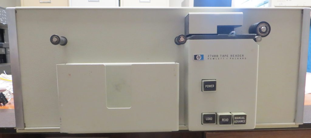
An denizen of the Classic Computer mailing list approached me recently about getting some paper tapes read in. These were BASIC programs from his High School days. At first I tried reading them in my PC05 paper tape read on my PDP-11/34, however that reader has a sprocket feed, and no good place to hold a rolled up tape. I tried 3D printing a spool reel holder and output guide, that that was not successful. So I decided I would try instead to use one of my two HP 2748 paper tape readers – an HP 2748B in particular.
Note that this reader has a capstan (small cylinder to the right) and a pinch roller (the larger black roller to the right) to firmly grip the tape and pull it through the read station. It works pretty well, but I do have to clean it frequently when reading oiled rolled tapes or they start to slip. Fortunately, both the capstan and the pinch roller are metal – no chance for rubber rot turning to “goo” here!
The Arduino “Sketch” described in this post, the PC side perl script, and some perl script tools for working with paper tapes for 8080 machines, PDP-11 and PDP-8 are available for download.
The jig I used to install new grain-of-wheat lamps into the read head is available on Thingiverse .
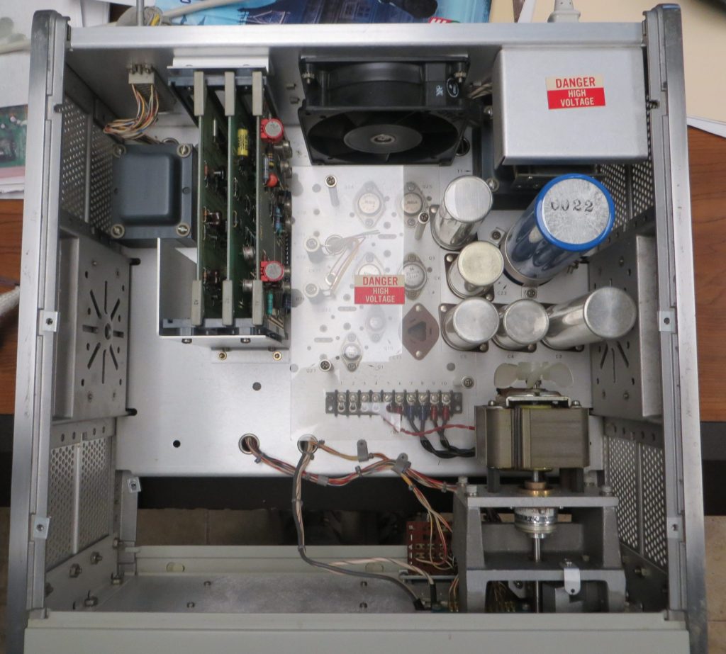
Like many/most HP devices, this device is absolutely gorgeous inside. Gold plated printed circuit boards (the entire board, not just the contact fingers), lots of space to work inside, easy disassembly and reassembly.
Top view of the HP 2748B Paper Tape Reader Chassis
A Continental Connector for the Interface
The first challenge was the connector. It is a 50 pin connector originally made by Continental. First I bought a Winchester connector off of eBay, but its pins were much too narrow. Then I purchased an AMP connector of eBay, and its pins were just a little bit too narrow. For now, I added solder to the relevant pins to ensure they make contact. Some are still a bit too wide and need some filing down so the connector mates fully, but it works well enough, for now. I will not be leaving this connector attached permanently because of the solder. But I thought it was a better than the alternative of wiring up a second interface connector.
The default logic voltages for the interface are +/- 12V. However, HP also planned for a TTL logic level interface (0 – 5V) by adding a clamping circuit on each interface connection. This clamping is activated by connecting interface pins C and H. Unfortunately, my AMP connector had a coax connector on pin C, so for now I made this connection internal to the reader. When I get some time, I’ll se if I can swap pins so I can make this connection in the way the designers intended.
My plan was to use an Arduino to drive the paper tape reader, and connect to that via TCP/IP, similar to how I did my paper tape simulator.
It’s ALWAYS a Light Bulb
The first thing I did was re-form the capacitors. This turned out to not be necessary. For one thing, most of the power supply capacitors are rated at 5 TIMES to 10 TIMES the expected voltage across them. There was almost no current flow after a minute or two of “reforming”.
The next thing I thought of (thankfully) was to check to see if the illumination in the read head was OK. Well, of course it wasn’t (though the lamps in my other HP paper tape reader, an HP 2748A, turned out to be OK).
Unlike the DEC paper tape readers, these HP readers use a grain-of-wheat lamp for each channel: 10 lamps in all, 8 for the data channels, one for the feed hole, and one additional lamp used for temperature compensation. Clearly at least one was bad, but it turned out to be much more confusing than that.
I had some lamps on hand that are ostensibly for an RK05 positions sensor, but when I tried to replace the lamp I thought was bad (and at that point, I thought it was just one), another one seemed to fail. I took out the lamp I thought was bad, and tested it – and it seemed OK. Put it back in, and it seemed bad. Eventually I figured out that what was probably going on was that the wires on the lamps were so corroded that solder wasn’t taking properly to the leads. Eventually I decided to order some likely replacements off of eBay and replace all of them.
The process of lamp replacement is sufficiently tricky and time consuming that HP service people generally were not expected to do it in the field. The bulbs aren’t listed as replaceable components. Instead, service people / customers were expected to acquire a replacement for the entire read head.
Metal alignment pins at least make the removal and re-installation process relatively straight forward – takes about a minute.
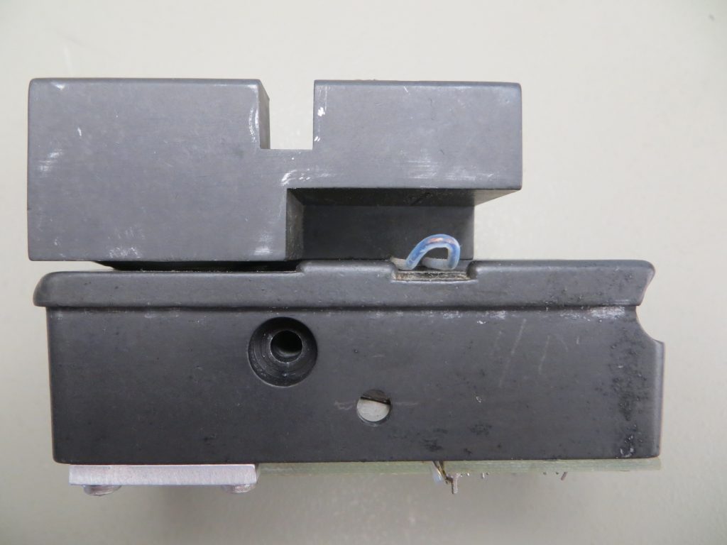
HP 2747B Paper Tape Reader Read Head, Front ViewHP 2748B Paper Tape Reader Read Head, Top View
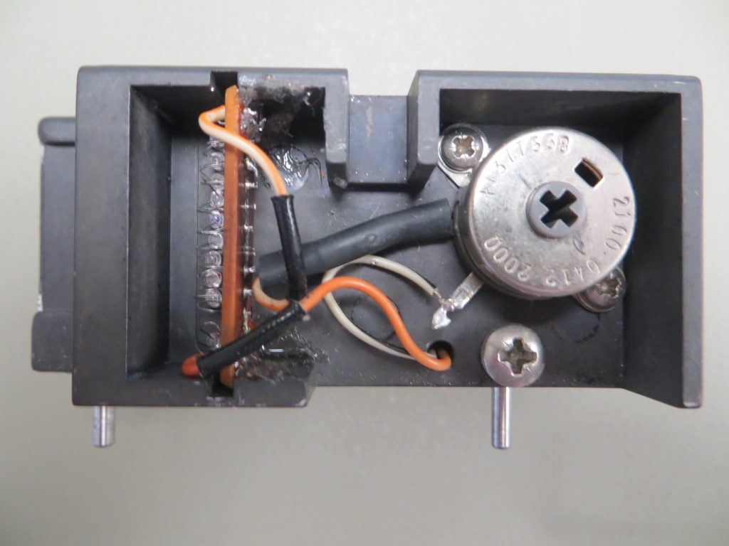
To do the replacement, I removed the little PCB (left side of the photo), unsoldered everything, including the wiring to the rest of the read head, and install new lamps. I had already learned from experience that getting a single lamp into position could be tricky, so I didn’t relish trying to do what with eight of the little wee beasties. In order to assist the installation, I made a 3D printed jig that fit the boards and had a place for each bulb at an appropriate distance from the PCB based on the lead lengths of the original lamps that I had removed.
It still wasn’t easy – at 70 years of age I am pretty shaky at times (and have been more shaky than average my entire life), but it worked well enough. However, since these bulbs are slightly different than the originals, I ended up adding a fixed 1/2 Watt resistor to add some additional resistance. That resistor is inside the black heat shrink tubing that goes from the adjustable resistor in the top view over to the PCB.
Then I used silicone sealant to hold the board in place, much as had been used originally – messy, but effective.
Adjustments, Adjustments
Next, I adapted the “solder enhanced” AMP connector to the tape readers interface connector. That took some trial and error in terms of how much solder to add so that I had good reliable contact. It still isn’t perfect: some are a bit too large right now.
Then I was ready to adjust the read head. Fortunately, there are good instructions in the manual (see the link at the top of this post) for how to do that. I ended up going thru that process several times, but in the end it ended up about where it was after the first time.
During this process I was also able to verify the interface signals were behaving as expected. It took a minute or ten to figure out that the read hole signal would not be present unless the READ button on the reader was engaged. Also, at first, I misunderstood the lamp/bit order – on this reader the feed holes go nearest to the front panel when inserting from left to right – the opposite of a DEC PC-05 reader.
The Arduino Interface
For this application, an Arduino Uno had sufficient interface pins, and unlike the Raspberry Pi, is supports 5V interfacing. The code was relatively straight forward, and uses the same kind of program I used for the paper tape emulator I called out earlier – the PC just makes a TCP connection and sucks up data.
The interface pins for the HP Connector, the Arduino and the Arduino digital signals are all documented at the top of the code, and symbolic constants and macros are in place for handling the Arduino port setup and usage.
There were some things I learned/ tweaked along the way:
At first I tried to stop the reader every time I sent a buffer of data to the PC. However, the clutch and brake on the reader don’t seem to be working quite well enough for that to succeed, so in the end I just streamed the data an “hoped” the Arduino and the TCP connection would keep up – and it seems that they do.
Originally I though I might have some kind of header on each buffer of data I sent, but it occurred to me that TCP is essentially doing that already. The code for that header is in SendBuffer(), but is commented out.
I was having problems with some extra characters, so I added a little time wasting loop to more or less ignore rapid transitions on the h0le signal. That code could probably be improved upon.
It is Working – Trust but VERIFY
After a couple of passes of tweaking the lamp positions and going through the adjustments, the reader reads a DEC test tape pretty reliably – maybe 1 error every 50,000 characters. It also handles both fan folded and wound “round” tape spools well. However, I always try and verify that tapes read correctly, so I wrote some perl scripts to do things like:
Verify 8080 binary tapes (the format is documented in the script)
Verify 8 Bit Intel HEX tapes
Verify Even parity text tapes
Verify PDP-8 binary format tapes
You can download a Zip archive with these tools, the Arduino Sketch and the PC side Perl script here.
One More Problem – There’s Always at Least One
As I started reading in tapes, starting with the DEC test tapes (MAINDEC-00-D2G2-PT and MAINDEC-00-D2G4-PT) things were fine. As I proceeded to read in some 8080 binary tapes, I started having some issues with the high order bit. That was easy to fix – the lamp was slightly miss-aligned.
I also found finding the balance between not having data errors (dropped bits) and having duplicated characters a little tricky – it took me a few passes doing the adjustment procedure described in the HP manual to get it working well.
However, I then discovered one more problem. Sometimes it would drop some of the null characters appearing in a blank area of tape after the initial leader. The HP 2748B has a special circuit that causes it to intentionally drop leader nulls – once you hit the READ button, it drops nulls until the first character. After trying this and that (including running through the adjustment procedure yet again), it occurred to me that maybe that circuit was firing, causing the reader to drop nulls.
I connected several signal lines to a connector that I thought might be useful in order to scope them (and not have to keep moving the scope probe around the board, as I have no extenders for these connectors), and quickly confirmed my suspicion. I tried a lot of things – including swapping some of the four identical transistors (two for a flip flop, and two more acting as signal inverters) so that the flip flop would have matched transistors, to no avail. I also tried replacing the capacitor that connects to +12V that resets the flip flop on power up (in case the READ button is already pressed). Nothing seemed to help.
I noticed on the oscilloscope that the length of time before the circuit fired when it shouldn’t was kind of random. Could this be noise? Connecting a .1uf bypass capacitor on the +12V line feeding the reset circuit was the first thought, but that was going to be harder to do on the board than I preferred. In the end, I hooked up the capacitor from the base of the reset signal inverter Q13, and that cured the problem.
Now the reader is generally reliable so long as I keep the read head, capstan and pinch roller clean.
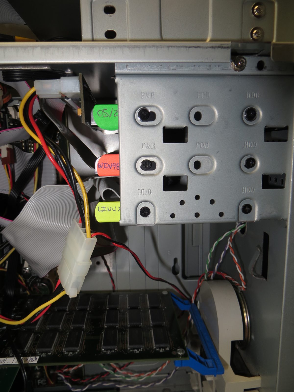
In early 2021, I converted the hard drives in my Pentium II computer which hosts my P/390E IBM mainframe processor card, which I call “Floppy Copy“. This machine boasts three different operating systems. Two are in support of its primary mission for copying floppies: Linux to host my Catweasel board (which may not see much future use, now that I have a Greaseweazle board), and Windows 98 for copying floppies using tools like IMD. It also has OS/2, in support of the P/390 board.
First some background: OS/2 had always acted a little wonky: I did the partitioning under Linux because OS/2 didn’t like to partition the 200GB drive. And then, having partitions of 2GB, 57GB, 57GB and 57GB, running OS/2 chkdsk on the last two 57GB partitions would sometimes clobber the first 57GB partition, for reasons I never understood – until I undertook this migration. (I still don’t quite understand why it never managed to clobber the 2GB FAT partition!)
So, off to Amazon I went, purchasing IDE to SATA adapters. The two from Startech and Kingwin worked fine. One from Sinloon worked, and the other did not work at all. In addition, I found, strangely, that the adapters would work with a 240GB drive, but not a 120GB drive. WTH?
So, then I went looking to see if the BIOS might be involved, and I found a BIOS update from Aug-17-1999 to Sep-09-2000. That cured the 120 GB problem. But then, in testing, I ran into the same kinds of issues on the 240GB drive I had seen on hard drives, with corruption after running OS/2 chkdsk.
Well, it turns out that this particular motherboard, a Chaintech 6BTM, has Ultra DMA-33 IDE ports –and only supports drives up to 137GB. Ahhh, so that was the problem.
I wanted to give OS/2 (and the P/390E) as much space as possible, so it got one 120GB drive. I tried and tried to move the drive partitions for Windows 98 and Linux over to a shared 120GB drive, but without success. The minute I created a second primary partition for Linux, Windows 98 would no longer boot. So, I simply imaged Windows 98 as is to a 120GB SSD (using only a fraction if it), OS/2 to a 120GB SSD and Linux to a 240GB SSD – because I already had it, having purchased it from before I learned about the 137GB limit.
Pentium II with SSDs for OS/2, Windows 98 and Linux (IDE to SATA adapter on OS/2 drive)
Only one of the three adapters I had supported IDE master/slave. The other two had to be alone on their cable. I am using one of those two (Kingwin) permanently.
Having gotten things tested, I went about testing the IDE to SATA adapters one at a time in order to write reviews. While testing the Kingwin adapter, though, I decided to plug it in with power on. Unfortunately I had the power connector upside down, and as soon as it touched, the computer dropped power. Worse, I could not then power it on at all — completely dead. Ohhhh nooooooooo!!!
After unplugging the power cord for a couple of minutes, I could at least try and turn it on, but it would not start up – no beep, no nothing. Fearing the worst, I tested the power supply voltages – all fine. Ohhhhhh noooooooo!!!
After 10 minutes of panic, I started testing cards from that machine in a reasonably close relative, my AMD Athlon machine with an ASUS A7M266 mother board. Video card: good. IBM P390/E even passed its diagnostics. (Whew). So then I pulled all the cards out of the Pentium II as well as the IDE to SATA adapter I had been messing with at the time of the infraction, and the machine came to life!
I put all the cards in one by one, and stopped at the POST test. All good. Then, just for giggles, I hooked up that last IDE to SATA adapter – dead in the water, apparently fried. Embarrassing: I fried an adapter. The good news: it costs less than $10. Glad I purchased four of them. (I kept the Startech out in reserve because it is the only one of the four which worked and can be set for Master or Slave.)
Having discovered that the P390/E was happy in the AMD with the A7M266 motherboard, and that the motherboard has OS/2 support as well, so in May 2021 I migrated the P/390E to the AMD machine, and upgraded to OS/2 Warp 4.52, so now I have support for the full 240GB SSD.
No, not that kind of “quickie”. Instead, it is about Volume V of the ALDs – now tested – in just over a week! This was due to a couple of related factors. The first 30 pages were address registers – continuation from the end of Volume IV. Then after a few more pages, the memory address register pages were up.
The second factor was a new testing technique. For cases where there are and or and/or or or gates that are similar (fed from a character of storage or another register), I started using a test vector generated from an integer counter, and then checked the results using straight-forward logic equations derived from the Instruction Logic Diagrams (ILDs), which allows me to zoom through those kinds of pages.
I also evolved how I test control signals. I typically don’t test those exhaustively with a loop (especially when they feed a latch or trigger), but I started a copy-paste routine with the variables that lets me build the tests a bit more quickly.
I really wish VHDL had a macro facility or call by name (or reference) capability, though, so I could write procedures that modify signals in a test bench. It would allow me to write generic and, and/or and or tests for various numbers of variables. Sure, I could generate the HDL with an external program, but that would actually take more time than the copy/paste technique I am currently using.
Volume V is the first volume that uses NOR (primitive DTL) for actual logic. NOR logic also shows up in gated input interface signals, but that is a different animal. I was only about 90% confident of my interpretation of some of those circuits, but so far they have been spot on.
Volume V did present a few challanges. First, another missing page: page 14.18.04.1, part of the zone adder, was missing in action. It was clearly a copy/assembly error when the drawings were assembled – page 14.18.05.1 appears twice on both sides of the same sheet: one of those shoud be 14.18.04.1.
Now, I could easily have just replicated the ILD as equations, but I took it a bit further than that, consistent with what I have done on other missing ALD pages. Research based on the card location chart uncovered that I had one card at 11C3A16 (type DEV) entirely dedicated to this page, though the chart only showed four of the seven gates on that card actually being used. I also discovered that the card at 11C3A17 (type DFS) had 3 gates dedicated to the cause and by elimination of a gate or two that appeared on other sheets I was able to determine which gates/pins were “available”. I struggled for a day to make it work with just 6 gates (3 from the DEV and 3 from the DFS) but I couldn’t find a way. So in the end I drafted the remaining 3 gates from DEV (which are a AND/OR triad) to complete the task. While this doesn’t agree 100% with the card location chart, who is to say that the card location chart wasn’t quite right. 😉
I did find a couple of ILD errors in this volume. On page 17 of the ILD, relating to ALD page 14.30.06.1 a couple of signals are inverted and depicted as feeding OR logic. In reality, these signals are inverted on the inputs (-Y – negative active) and ANDed together. It happened because that ALD happens to depict a single NOR gate as two – one feeding the other – because that card has more inputs than can fit on a single logic block in an ALD. The symbols on the gates on the ALD do indeed imply that all the inputs are ANDed together, but if one didn’t spot that both blocks involved are the same card gate, one could easily misinterpret it. Curiously, the same thing happens on page 14.30.05.1 (the previous page), but in that case the engineer who prepared the ILD interpreted it correctly.
Those same blocks on those same two gates allowed me to leverage a feature on my application. When I entered those logic blocks, I realized that they were, in both cases, the same gates. However, since they are next to each other on the ALD they were not candidates for using the “extension” capability to combine them – there would have been room for that on the page, but they were not depicted as extensions. So I moved the inputs from one of the gates of the pair to the other, and removed the output from that first one as well. When I first tried generate the HDL, the application noticed the unconnected gate and generated a (harmless) error. However, a while back I added the ability to tell the application to ignore a given logic block when generating HDL. Worked like a charm.
Another case where I ran into that sort of thing was on the real time clock, where a given switch “deck” was split in two, and also the block title — which I used to generate the name of a switch signal — was replicated between decks. In order to generate this correctly I had to tweak the logic block titles to separate them, and join the switches together in the test bench.
The ILD’s also, generally, did not include the gates for address wraparound from x9999 to 00000 for 60K and 80K – only for 20K and 40K machines. The wraparound logic was present on the ALDs however, and was easy to decipher. (Wraparound for 100K is automatic because there are only 5 digits of addressing. 10K machines to no support wraparound at all, if I recall correctly)
I discovered a typo on a signal name on page 14.17.10.1 “-S AR BUS GRD OUT THP0B” — GRD should be GTD (gated).
ILD figure 24 had an error relating to page 14.16.04.1 om calculating the Address Register Exit Channel “C” bit – at the least it didn’t match the ALD. In general I defer to the ALD after carefully checking the logic, figuring that the ALDs are later in the timeline than the ILDs.
I also found a case of a misleading signal name, where the signal name implies two factors in an AND, when there are actually three. However, going back I can’t seem to find it – I will update this page if I come across it.
Finally, I have come to dislike a certain idiom that has appeared on a handful of sheets, where a pair of latches are ins sequence, usually named “… Control” and “…” where the output of “…” resets “…Control”. A real pain to devise a test bench.
Came across something interesting today on Automatic Logic Diagram 13.50.04.1. It refers to unit “8” – which is for punch column binary – a special feature. An 8 character is just the 8 bit – odd parity. However, to decode unit 8 per the ALD one would have to have B 8 – and no check bit – even parity- which can never happen. So, if one were going to have the column binary feature installed, it would require an actual rework to change the input to one of the pins on ALD 13.50.04.1, coordinate 3A (11DJ02) from “+S E CH U SEL REG B BIT” to “+S E CH U SEL REG NOT B BIT”. So, without this rework, the machine would simply not decode unit 8 at all – perhaps intentionally. (Of course, on the generated version, this would be an easy fix, but for now I just left it as is.)
I have been testing the logic generated from each Automated Logic Diagram (ALD) page, using the Instructional Logic Diagrams (ILD) were available to guide my testing. Until today I don’t recall finding any cases where I actually made a connection mistake when I entered the ALDs into the database – until today. On page 13.50.01.1, I had mis-substituted signal “-S I-O Lozenge Latch” where I should have had “+S Logic Gate E 1” as the input to the gate at coordinate 5H. The testing caught it.
When I entered data for each sheet, I tracked usage of each signal count. I had a “2” written next to “+S Logic Gate E1” — as I should have. I must have missed that when I checked the signal usage counts after entry (“-S I-O Lozenge Latch” had the two instead). The latter is right below the former on the left side of the ALD, which made the mistake not unlikely, and made it easier to mis-interpret where I had written the signal count of 2. I even circled the 2, meaning I checked it. Oops.