
So, not the yummy treats, but a new problem that showed up with the SAR instruction.
The fix to ERR 60J was pretty easy. That was a gate for feature S10 – a 10K 1410 that needed removing (and its output replaced by a logic ‘1’) on page 14.30.05.1. QED.
However, after fixing that, I then experienced an error near another Store A Address (SAR) instruction, at (just before) location 8624, exhibiting A Channel, Assembly Channel and Address Exit validity checks, with garbage in the B Address Register. However, when I ran the same instructions in the same place in the address space (but with memory otherwise all blanks) it seemed to work just fine. How could this be?
The first blind alley was either that the print chain used for the diagnostic listing printed the 1410 characters “?” and “!” as “&” and “-” respectively, or there was a bug in the listing version that was fixed on tape. So much for that hypothesis.
To figure this out it would be best if I could get it to fail under simulation (There is a scoping capability in the FPGA as well – but not as quick and easy to use.) As mentioned above, during initial testing for this problem, I just loaded the relevant instructions into the appropriate memory locations with memory from 10K up to 40K being blank characters and the failure did not occur. Further more, during testing I discovered that if I had only loaded the first 10K of the 1410 1401 mode diagnostic, M011, as the listing only went up to just under 9K, this problem also did not occur, and the only error ?3S (translated into address 07032). However, that diagnostic is ordinarily loaded from the 1410 diagnostic program TC50, and when I used the image that I have that goes up to 40K, all heck broke loose with the error noted above. I then changed my memory initialization to all ‘9’ characters aside from the instructions under test and was able to reproduce the issue under simulation.
This led me to an initial suspicion that something must be causing more than one B character register from “core” to read out simultaneously. Only one is supposed to read out at a time – and their outputs are OR’d together. If more than one read out at the same time, the results would be problematic. But how was this occuring?
After many simulation runs looking at various signals and what might be going on, I finally hit upon this one.
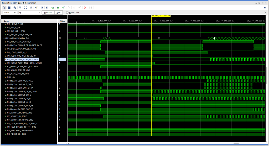
Looking at the timing diagram one can see signal -Y MODIFY BY ZERO essentially “oscillating” starting shortly after 30.153 milliseconds. That in turn caused the Ten Thousands position to change quickly, resulting in the issues as that position is used to select among the B character registers from memory. That latch “oscillation” then in turn set up problems all over the place, particularly in the Address Channel.
Looking again at the same timing diagram, one might notice that +S ADDR MOD SET TO ZERO and +S RESET ADDR MOD CTRL LATCH are both active when +S RESET ADDR MOD LATCHES becomes inactive. Those two signals both impact the Modify By Zero CTRL latch at blocks 3A and 2A of ALD page 14.30.09.1, resulting in the signals trying to simultaneously set and reset that latch – a pair of cross connected NAND gates – a typical R/S latch. This is a big nono.
In my ALD page generation, these latches are recognized, and “D” flip flops are added after each gate involved. So instead of being undefined, in this kind of situation a kind of “oscillation” is set up at about 1/2 the FPGA clock speed of 100MHz (which is also the memory clock signal “MB 0 clka” in the diagram).
The general approach I took to fixing this was to either a) prevent a set during a time when the reset signal was present or b) prevent a reset during a time when the set signal was present.
To try the first approach, I added the +S ADDR MOD SET TO ZERO signal as an input to get logic block at 3C on page 14.30.09.1. This was done directly in the VHDL – much quicker than puzzling out where to find/fudge a logic block to add to the equation and test – especially if, as in this case, the fix doesn’t work. So, apparently this situation really needed to do a Modify Address by Zero operation (which it did: this, like the previous problem, occurred while copying the contents of the A Address Register to the B Address Register.)
So, then I went to the other approach, (undoing the first one), which was to add the +S ADDR MOD SET TO ZERO signal in so as to inhibit a reset while it was active. That indeed fixed the problem, and the change to the ALD was very easy: all I had to do was add the +S ADDR MOD SET TO ZERO signal into the existing “wired OR” at ALD coordinate 4E, as “ECO” JRJ004.
As for the original 1410 implementation, this could easily be another case where the fast FPGA logic causes an issue that never cropped up in the real hardware.
After doing this, the diagnostic worked OK except for the ERR ?3S. (I have not yet tried the manual part of M011 – testing the sense switches, etc.).
Getting close…