
“There you go again”
What with the Thanksgiving holiday and all (even though it was spent at home, ’cause 2020), it took several days to ferret out the issue where simulation of a power on reset followed by START worked, but on the FPGA that failed. Of course it was bound to be an issue with triggers. However, I used the Integrated Logic Analyzer (ILA) to confirm that issue before I changed anything. Sure enough, card type DEZ needed the same adjustments as DEY: I changed it so that the transition of the AC SET input was required to occur after the transition of GATE ON / GATE OFF. At the same time, I moved all of that logic inside the FPGA clock transition section, to make it synchronous with the FPGA clock. That fixed the issue, which occurred on page 12.12.31.1
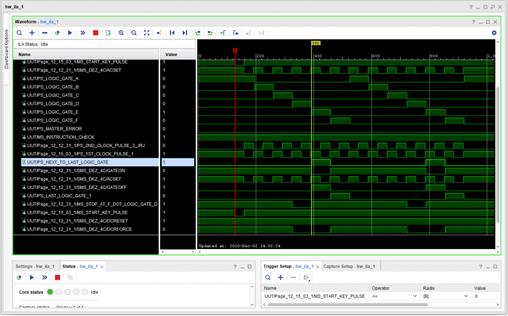
So now, after I load the FPGA, all I need do is press START and I see the correct waveform. (Also note that the transition of the output to ON (NEXT TO LAST LOGIC GATE) immediate turns off GATE ON – because that is exactly how it is wired. So first we see -S (active low) STOP AT F . LOGIC GATE D at about 320 into the trace. Note that GATE ON is already present, however, the trigger is held off by the “DCRFORCE” input coming from block 3B until STOP AT F . LOGIC GATE D goes true. Next, we see CLOCK PULSE 2 appear (but it gets inverted before it us used for ACSET, so it essentially matches CLOCK PULSE 1) at 389 on the diagram. Then at 392, the trigger sets, NEXT TO LAST LOGIC GATE goes true, and GATE ON is removed.
Decoding Memory Addresses
The IBM 1410 storage address register (STAR) is a five position two-out-of-five code register. However, it is not used altogether to select an address. On a read, all of the 10,000 position core memory segments are read, in parallel, each to its own B data register position. So, for a 40K machine, it has 4 B data registers, for 0-9999, 10000-19999, 20000-29999 and 30000-39999. On a read, the ten thousands position of the memory address is used to select one of the B data registers to gate onto the B Channel. During the write portion of a memory cycle (to change memory, or to regenerate memory if only a read is required), the ten thousands position is used to decide which B data register to update, if any, before the write portion of the memory cycle. The other B data registers retain their original contents from the read cycle.
At present, rather than simulating the full core plane of the IBM 1410, I chose to implement memory, for now, using a binary address and (probably) an array of 10K FPGA Block RAM segments. This means that the binary addressed RAM for the FPGA IBM 1410 uses a 14 bit address (to cover 0-9999), with memory arranged in the same 10K sections.
The inputs into this decoder are the -Y MEM AR UP/TP/HP/THP signals, which are in two-out-of-five code. The output from the decoder is a 14 bit binary address, 0 – 9999. This was implemented “brute force” by decoding each of the positions to the appropriate binary number, so the UP decodes to 0 – 9 in a 14 bit binary number, the TP decode to 00 – 90 (by tens) in a 14 bit binary number, and so on. Then the four binary numbers are simply added together in the VHDL – leaving the implementation of the adder for the tool chain to figure out.
Memory – and a Startup Issue
Next I created a simple set of Block RAM modules (BRAM) along with a VHDL wrapper for the 40K main core unit, accepting the aforementioned addresses in 2 out of 5 code, the Ten Thousands position (so that eventually it can tell if it is the 40K main core or the 60K Z Frame core), inhibit signals, and output sense signals. In order to more easily generate the necessary BRAM enable and write enable signals, I also brought out the MY_X_RD_1 and MY_X_WR_1 signals.
After some fussing I got my BRAM module working under simulation, but ran into an odd problem where during startup the system would overwrite location 00001 with garbage (and presumably 10001, 20001 and 30001 as well) because the system was left in Logic Gate B (LGB) state during the power on reset that then proceeding through a memory cycle once the power on reset was complete triggering the computer reset- thereby writing those locations with uninitialized garbage. (Computer reset will finish a cycle if it is encountered mid cycle to avoid corrupting core.)
I temporarily disabled memory writes, and then found I could successfully execute my halt instruction (WM/. WM/. in locations 1 and 2) under simulation AND on the FPGA.
The startup issue was interesting. I had supposed that the power on reset signal issued on ALD page 12.65.01.1 would start OFF, come ON during the power on reset, and then turn OFF again. However, that was having the undesirable effect of letting the system progress from LGA to LGB during the power on reset as mentioned above. Some study of the aforementioned ALD, along with the IBM 1415 console manual (the power on switch is located there) made me realize I had misunderstood.
That power on reset signal is asserted during power on to keep the system in a reset state (and thus in LGA) for an RC constant of about 500ms. Then, after that, the signal goes to logic 0, triggering the one-shot at block 2D to do a computer reset. At that point, the machine is in LGA, and the computer reset will leave it there.
Since I already have a system initialization VHDL process in the FPGA VHDL logic, it was easy to manage the power on reset signal there – indeed, the two may eventually become one, as they both have the same purpose of getting some stuff set up before letting the IBM 1410 CPU start.
This tested OK under both simulation and on the FPGA, though I have not yet verified that the FPGA is actually writing the contents back into the BRAM.
Next up: testing write by setting a wordmark somewhere (to verify read/write), and then halting, and a simple loop – both of which should be possible with my current VHDL by just changing the RAM initial values.
Update: The instructions sequence, starting at location 1, of setting a word mark at location 8 (which takes locations 1 through 6), a NOP instruction (reading out the set word mark instruction needs a wordmark on the character after) and then a period (halt without the word mark) behaves correctly. Wohoo! I have something of a CPU.
Next up: starting work on the console.