We just returned from France! We booked a cruise based on a mailing from the Wisconisin (the *real* UW) Alumni Association late in 2024. The cruise took place in October, 2025. We had a great time!
Overview
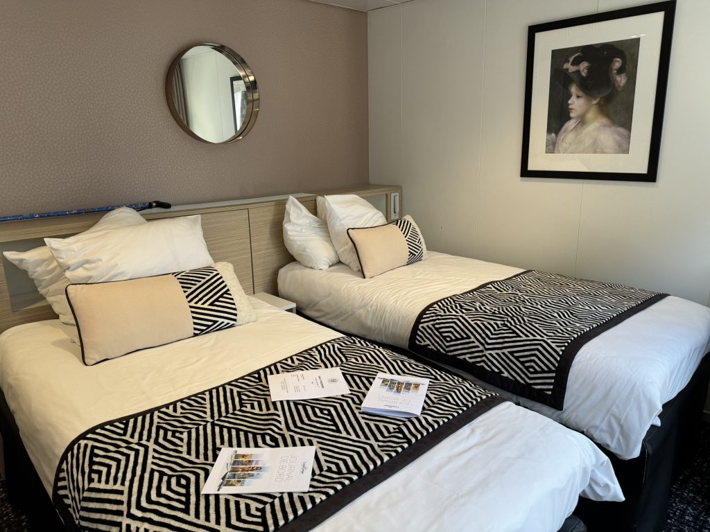
The cruise was organized and managed by AHI Travel (AHI), an organization operating out of Illinois, in coordination with the Wisconsin Alumni Association (WAA). Our trip started with a two day “pre trip” in Paris, followed by a 9 day excursion on the MS Renoir on the river Seine, oerated by CroisiEurope Cruises.
On the whole, the experience was delightful, with many great memories, detailed below.
The Cruise Staff
We had three “Travel Directors” on our ship, employed by AHI: Fred Burke, Reinhard (Rainer) Groeting and Signy Brink (more info on each is available on the AHI website). They were all wonderful and helpful during the trip, and were very understanding and helpful in tailoring the experience to accommodate my Gail’s currently limited mobility.
In addition, the WAA sent Melissa Zehner along on the trip, and she was also a great resource to have along on the trip.
More on the ship’s crew later.
A Shout-out to TSA
Yup – a positive report on our experience with travel security during the trip. When we went through security in Madison (TSA Pre-check), they discovered that this idiot (i.e., myself) had managed to leave a Swiss army knife in his briefcase. When they took my briefcase over for a more thorough search, that was not a big surprise – it had all my electronics, chargers, Lithium batteries, etc. inside. But the agent poked and prodded for quite a while, at one point asking if there was anything that I knew of that was sharp inside. I indicated that no, not to my knowledge, but after a bit more searching, produced my knife — with my name on it. OOOPS!!! It had been a gift from my wife a few years back, and I had moved it from my backpack to that case who knows when, and didn’t notice it, even when I first emptied that case and probed it myself before I started packing it up. The agent was very good about it, offered that I could go back, have the airline retrieve my checked bag (I declined) and then kindly confiscated the thing. No hassle, no barking, just doing his job to protect us all. Thanks, buddy.
And then, in Detroit, going throu security after our return flight from France, I noticed at the last minute I had not taken my FitBit and Apple Watch off and put them in my briefcase, as I usually do. So I then removed them and tossed them in the bin with my briefcase. But after I went through the metal detector and retrieved my briefcase, neither was in the bin — though my FitBit was in the briefcase side fold at that point (perhaps put there, perhaps by random chance). No Apple watch. I searched in a panic, but came up empty. At that point I decided to look for a TSA agent, but he was not at his desk at the end of the security check at that point. I waited, and looked again and there he was, holding my watch. I came up, pointed to it and said it was mine, and he returned it to me no questions asked. I unlocked it, and mentioned I had done so, demonstrating that it was mine. Again, no muss, no fuss.
And these guys are not currently even receiving their paychecks!
Days 1 and 2: Getting to Paris
We purchased the “Paris pre-trip extension”, and arrived in Paris one calendar day after we left, because of the long flight and a 7 hour time difference.
(Unfortunately, a couple of days before our scheduled departure, our 10 year-old washing machine broke down – so I had to do the laundry at a nearby laundromat!)
Dealing with Charles de Gaulle (CDG) airport was hard for Gail. First off, when we arrived, I had not noticed that we arrived in Terminal 2, sub-terminal M instead of the expected sub-terminal K, so got a little confused looking for immigration/border control. We ended up in the basement of “M”, and asked airport staff how to get to border control, and while they were very pleasant, they didn’t seem to know either!! A few departing travelers incorrectly suggested that we must have already gone through immegration to get there. Finally someone pointed us in the right direction, and after going up some stairs and/or elevators, reached the automated shuttle train stop. I was quite confused, because I though we were already in “K” when in fact we where in “M”, but at the last instant decided to hop on the train, and just as I did that, the door started to close on my backpack. I got on, but Gail didn’t. I shouted I would get off on the next stop (which is “L”) and did so. When the train arrived, I didn’t see Gail at first, but then spotted her, and hopped on to her train car. We then proceeded to “K” and got off.
MORE stairs / elevators and we finally got to immigration, aka border control. There we caught a break, and an attendant spotted Gail’s cane, and directed us to the priority line used by flight crews and the like. Five minutes and we were through – along with an unexpected entry stamp on the visa page of our passports – didn’t know folks ever did that anymore.
Then it was off to pick up our bags. Not spying an elevator, Gail managed like a trooper and took the stairs. Our bags were already on the carousel waiting for us. Picked them up and headed off to find customs.
On the way to customs I intended to exchange a smallish amount of dollars for euros, planning to use ATMs to get euros for later substantial gratuities for the travel directors and ship’s crew, but I foolishly let the attendant talk me into exchanging more. Ouch. Dumb.
Customs was a non-issue. There were guards there, but nobody asked any questions of anyone — and we had nothing to declare, anyway.
Next, it was off to find the AHI sponsored transfer to Paris. After customs I looked for them, but didn’t see their sign at first, so I parked our luggage with Gail, and went back and looked and found them. The staffer loaded our stuff onto the bus and off we went. It was a circuitous route from Terminal 2 to Terminal 1 to pick up some more fellow travellers – but there were only about five of us on a full size bus to get to the hotel.
L’Hotel Hilton Paris Opera
Nice hotel. Very nice indeed, with lobby decor appropriate to Paris – but otherwise quite American. The day we arrived, the revolving doors were not working, so the lobby staff / porters (and there were several) pushed to door to help guests. We had two full sized beds, side by side.
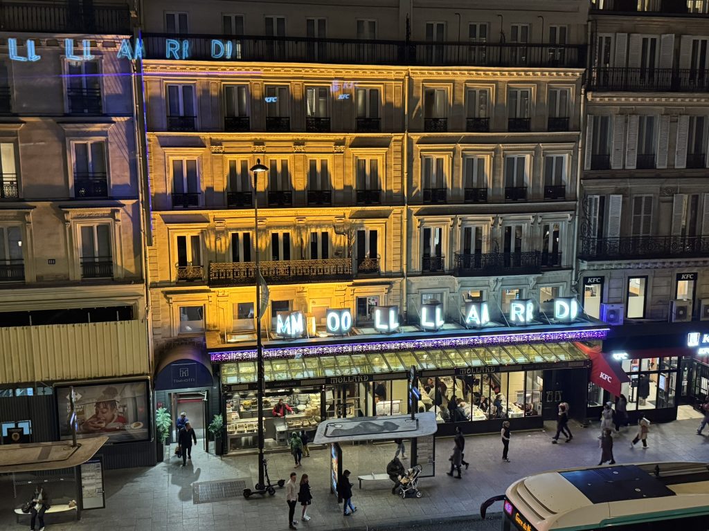
Our rooms were not yet ready, so we decided to go get some lunch. Signy suggested we try out Brasseries Mollard, across the street.
Breakfasts were a very good buffet, with a variety of foods available, including some pretty good pastries. They were included with our room.
Brasserie Mollard
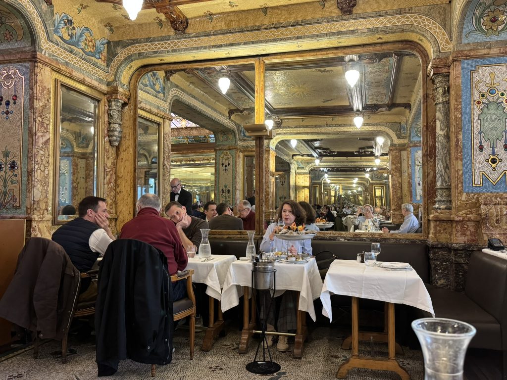
A “real deal” of a French restaurant. (You can see a reflection of Gail and me as she took the photo immediately above!) We arrived about 15 minutes before they started serving (which was good, but confusing for them and us), and requsted “une table pour deux” – forgetting that restaurants don’t typically open for “dejeuner” until noon. The maitre d’ was a little upset, and didn’t speak English, but finally got his point across by pointing to his watch saying (pretty loudly) “a midi” (at noon), to which I responded “je comprends” and we had a seat. Shortly a nice hostess confirmed that we were OK to wait and would be able to get a table.
When it was time, very shortly after noon, we did get a table, but it was clearly not a great location – it was a long-ish table, with a power cord for the lamp running diagonally over one corner.
At first the waiter didn’t seem to understand my request for “une carafe d’eau” and served me a bottle of water (which is not free), but later did bring the carafe over for us. The waiters were not snooty at all, and served us nicely. Speaking a little French certainly helps!
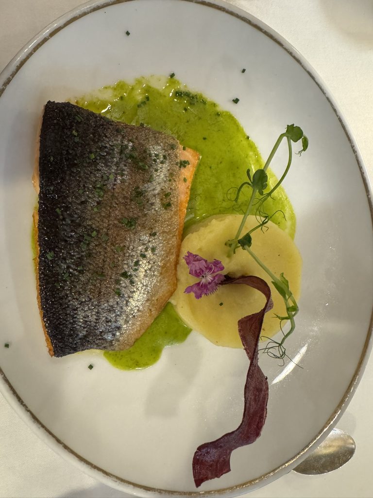
Gail had some salmon, and I had some chicken. Both were delicious.
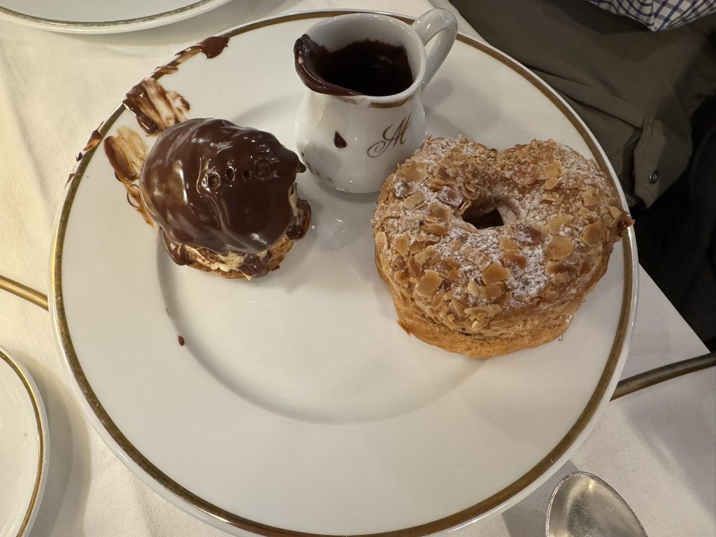
At the end of the meal, we had desserts. Delicious!
After our delicious lunch, it was back to the hotel – but our rooms were not yet ready. After a couple of checks every 15 minutes or so, I nodded off in a nice wing-back lobby chair. Signy came over and touched me gently on the shoulder to wake me, and then helped expedite the process of getting our room.
After lunch, and getting into our room, we crashed until a small reception for tour guests held by AHI in one of the hotel’s reception rooms. Afterwards, we decided to eat small, and went across the street to Brioche Doree, across the street from our hotel, which turns out to be a world-wide chain. They were nearly out for the day, but we had a turkey sandwich and a tuna salad sandwitch along with some chocolate eclairs. Pretty darned good for fast food from a tiny hole-in-the-wall. In the process, I discovered that one of my credit cards (the only one I had with me from the hotel across the street) wasn’t set up properly for France, and had to quick run back to get my other card to come back and pay. The restaurant was actually willing to let us have the food and come back later to pay.
Day 3 – Paris
After breakfast, the trip included a guided bus tour of Paris, hitting the expected spots along the way. Not so great for photos, unfortunately.
Then off to a guided walking tour of Le Marais district (literally, the marsh – as it was built on one). Gail and I parted company at the BHV department store. She and her newfound friend Tommie stayed behind and did some shopping, and then waited for us in a nearby cafe.
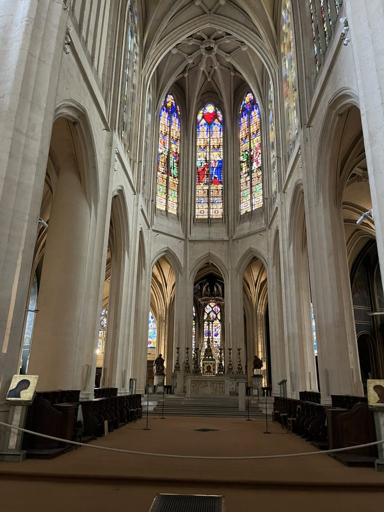
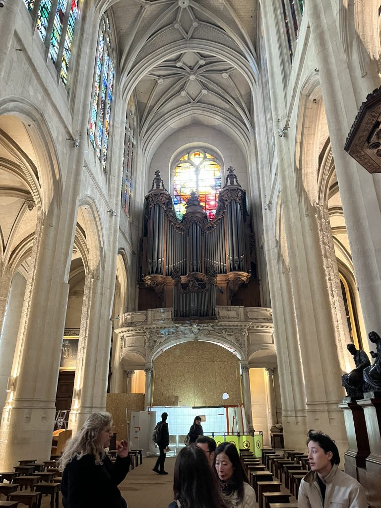
First stop was l’eglise Saint-Gervais-Saint-Protais – very beautiful, indeed:
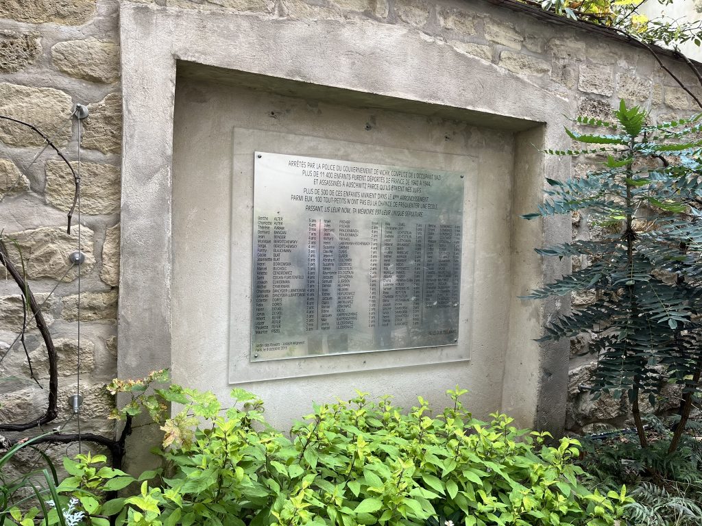
The tour also visited some monuments dedicated to the Jewish community that suffered greatly during WW II:
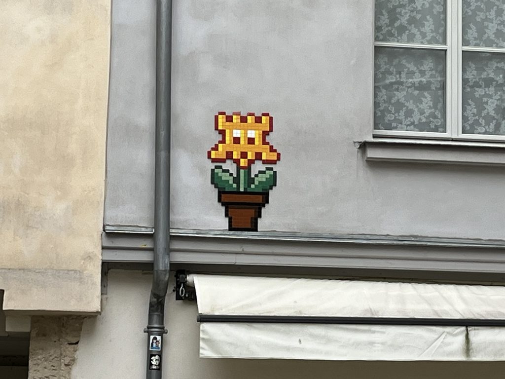
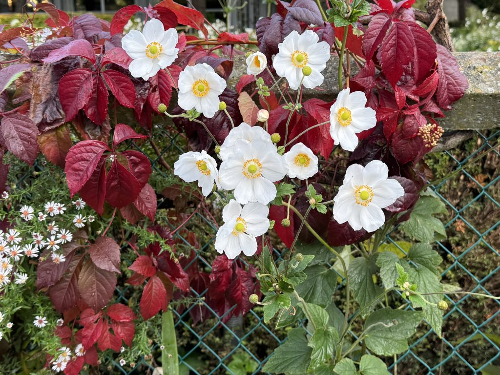
Also scattered about Le Marais were some 8-bit-ish pixelated images, apparently designed by an artist known as “Invader“. These can be found all over the world.
At the end of the walking tour, Gail and her buddy rejoined us, and we went back to the hotel, and had lunch at “Hippopotamus”, again, across the street from our hotel – which turns out to be a chain of grill restaurants.
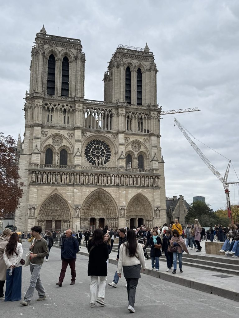
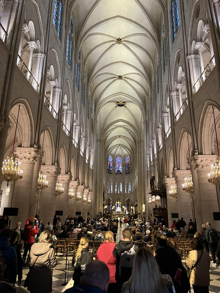
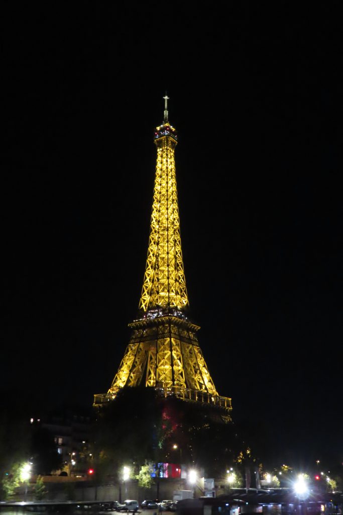
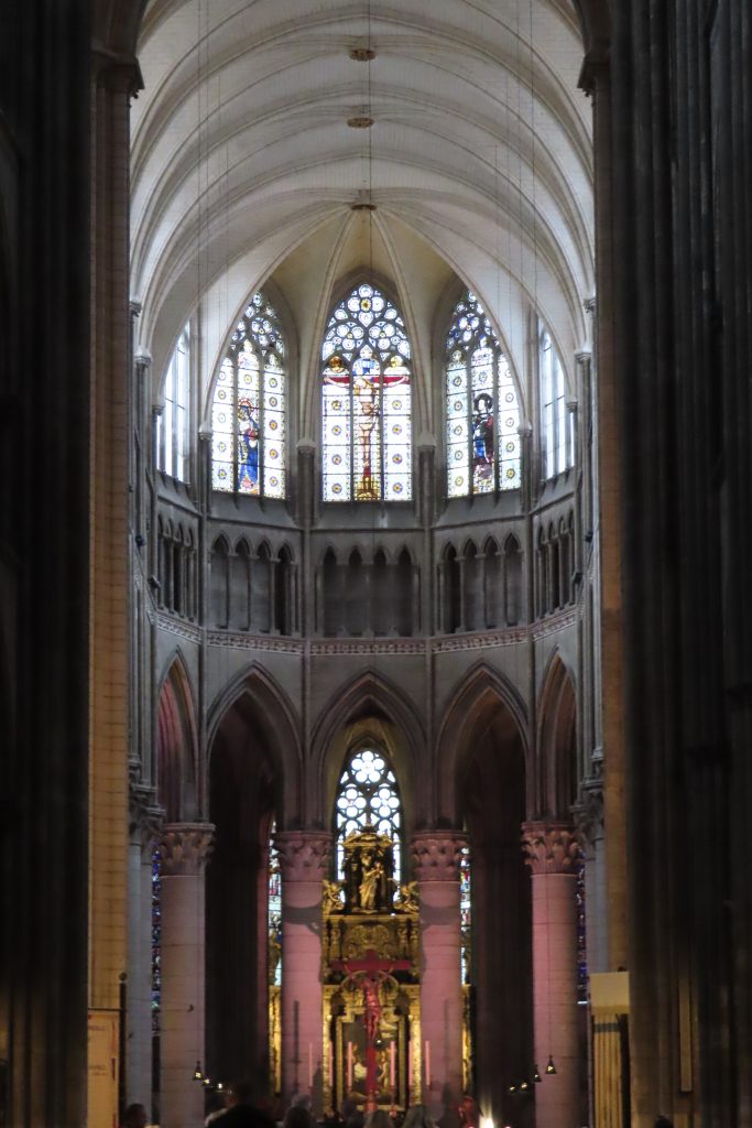
After lunch it was off to Notre-Dame. Getting the taxi was a little weird. The first two taxis and some customers appeared to have some small disagreement, and when we went to the third, he declined pointing ahead in the line. After a bit we came back, and by then he had realized that he was actually the front of the usable line, and we climbed in. The driver seemed concerned that we would understand that he had to go around the block at the beginning – I think he saw me looking at the meter – but I was not concerned at all. A short trip in traffic, and a standard faire of a bit under 30 euros, and we arrived at our destination: Notre-Dame de Paris.
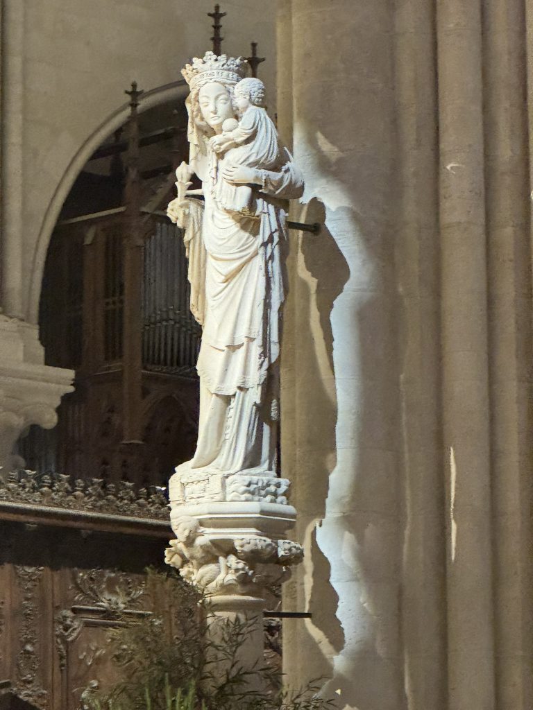
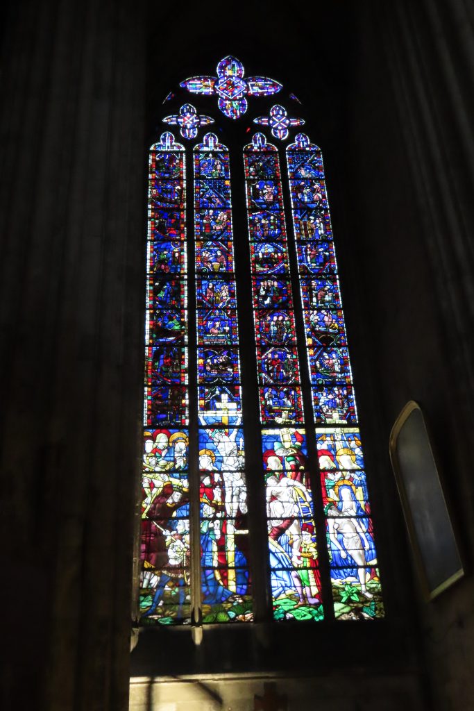
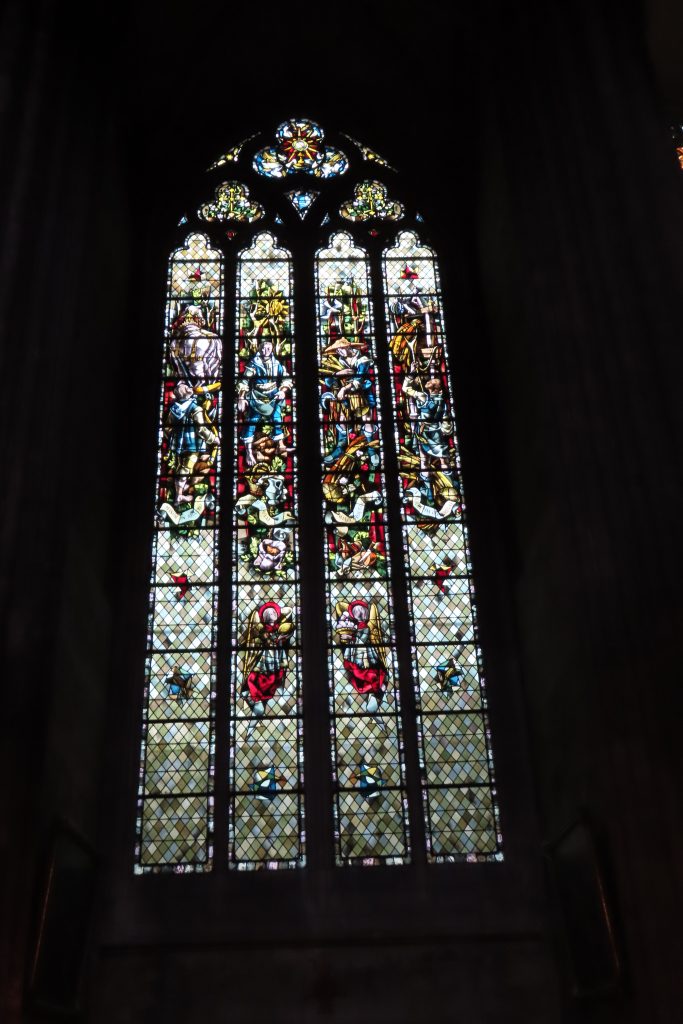
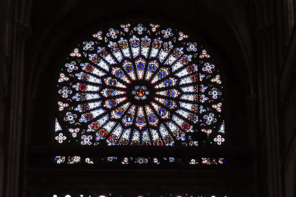
Being more of less off-season (though a vacation time for children), the line was short and moved quickly — but when the staff saw my Gail’s cane, they directed us to the no-line timed entry station, and we went in. We took some beautiful photos, and then attended Vespers. Very nice. As you can see from the first photo some restoration work is still in progress.
After Notre-Dame we were pretty hungry, so we grabbed some food at a little Italian place on a street near by, Cafe Leone. Just the ticket.
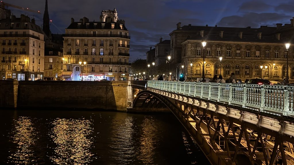
After that, it was time to find our way back, which turned into a silly adventure. It did not occur to me to open a map app to get to a taxi stand, we we took a wrong turn on the street. Finally we gave up and I flagged down a tax just coming off L’Ile de la Cite and we jumped in just around the corner. The driver didn’t speak any English, but I managed to communicate the name of our hotel, and a standard fare later, we arrived back and ready for bed. While she was waiting at the corner, Gail took this photo across the Seine back towards L’Ile de la Cite (you can make out a bit of Notre Dame in the background.
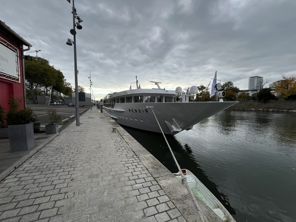
Day 4 – Embarkation Day and Paris By Night Sail
No time for touring, we had breakfast, and then packed back up and notified the porters our bags were ready, before checking out.
We had a very pleasant lunch at Cafe Marco Polo, once again, just across the street.
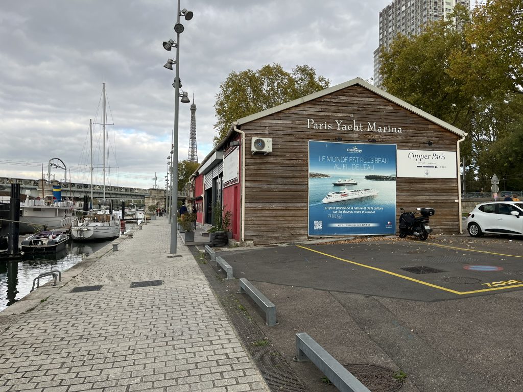
Then it was back to the hotel lobby to get our transfer over to the MS Renoir.
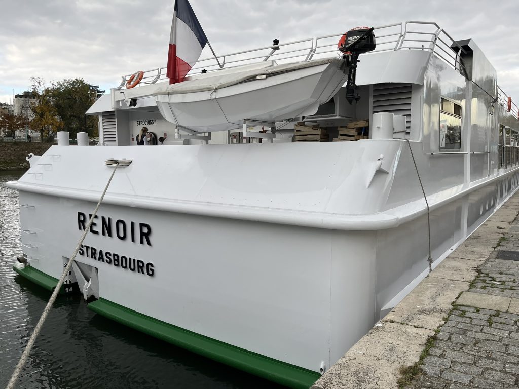
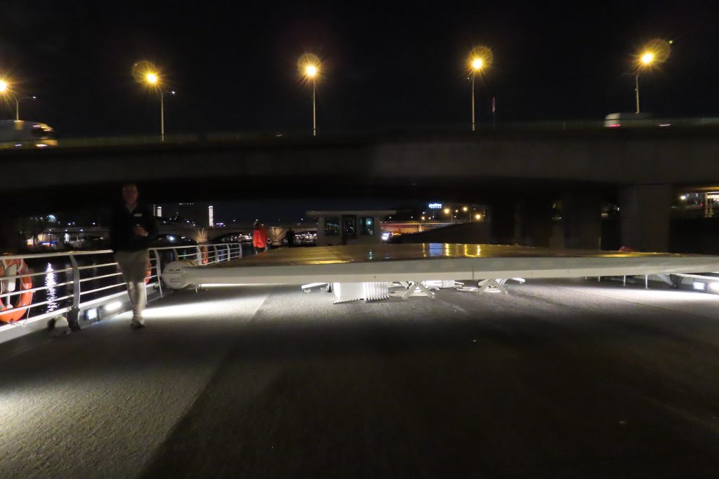
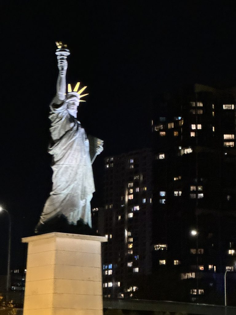
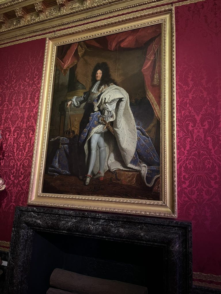
During dinner, the ship left the dock and sailed to the South and East – the opposite of our eventual direction, so that we could sail through Paris that evening. The bridges in Paris can be very low, and this ship is specially equipped so that the wheelhouse and the canopy for the passenger area above decks can actually be lowered down to deck level. The top photo shows the wheelhouse in its raised position. The photo of the Statue of Liberty in Paris below is quite fuzzy as light was low and the boat was, of course, moving…
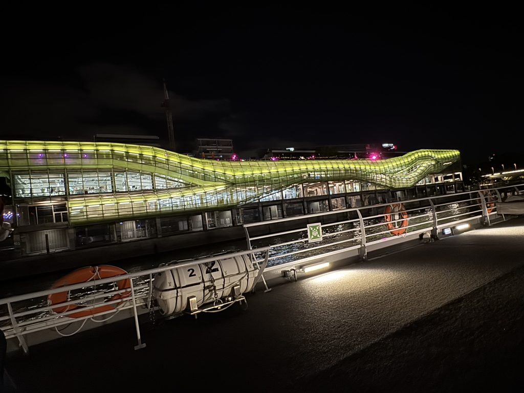
We said “au revoir” to Paris as the ship sailed on to Poissy.
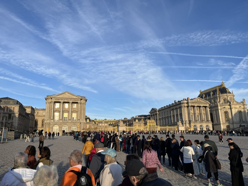
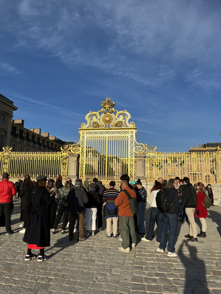
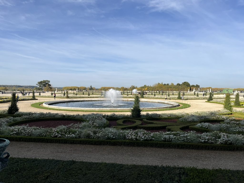
Day 5 – The Palace of Versailles
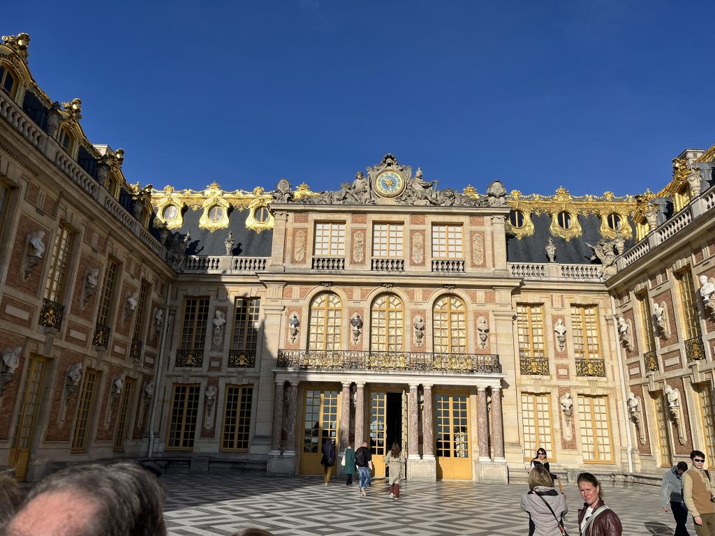
A first trip to France would presumably be incomplete without the obligatory visit to the palace of Versailles. But what a madhouse — and we were there “off season”. They used a timed-entry setup for groups, and we tood a long time waiting for our time (and then some), which was a bit difficult for Gail.
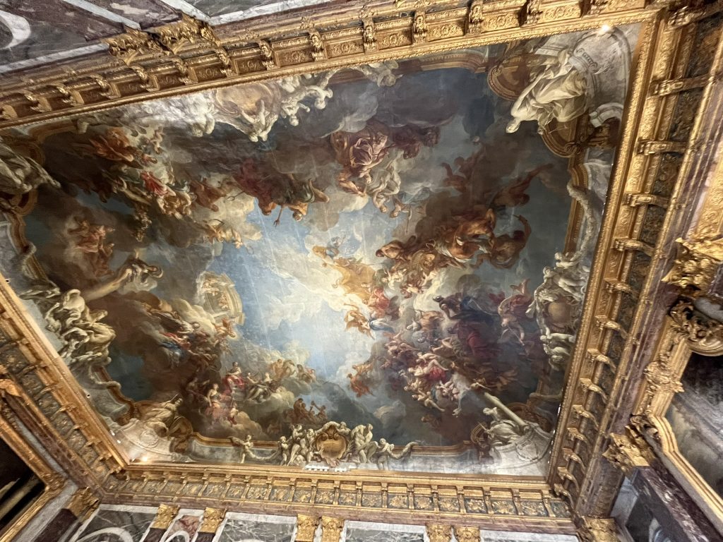
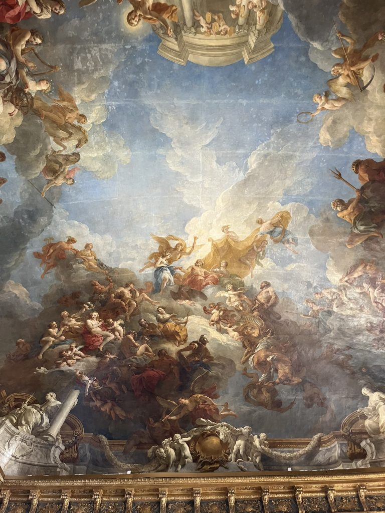
It was very crowded, so getting good photos taken was sometimes hard – we eventually decided to just go buy the book at the end (all tours end at the gift shop, after all.)
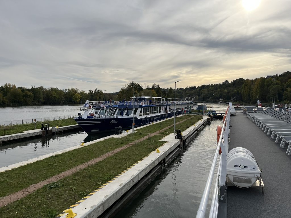
The rest of the day was spent under way, making our way to Rouen, navigating through some locks along the way.
Day 6 – Rouen and Normandy Abbeys
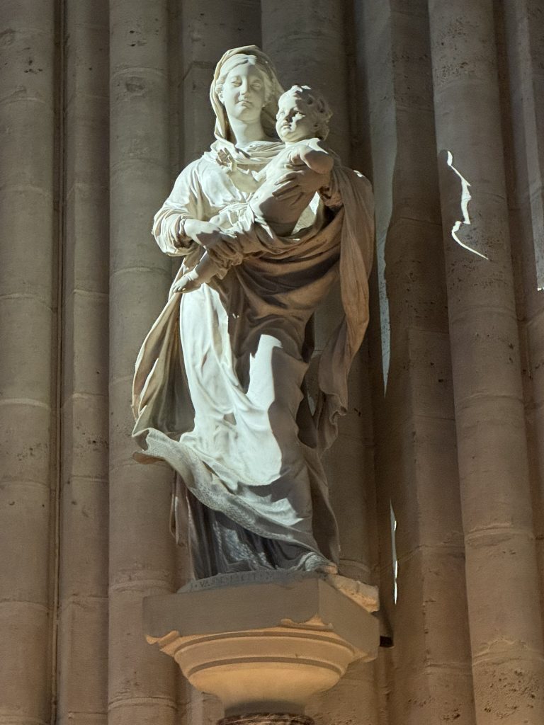
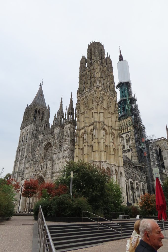
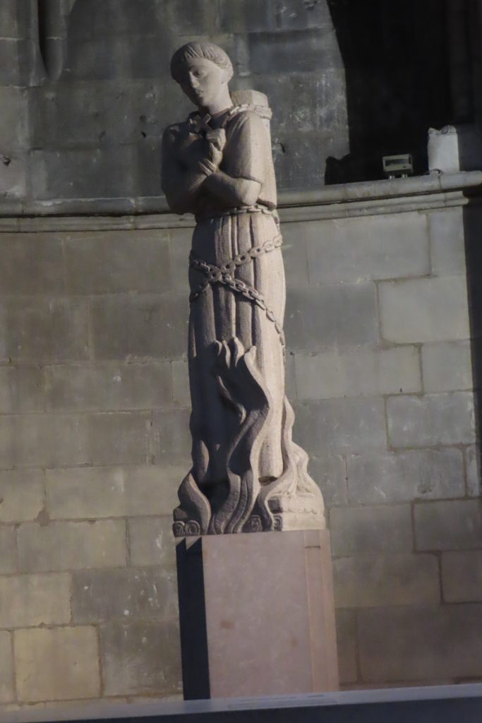
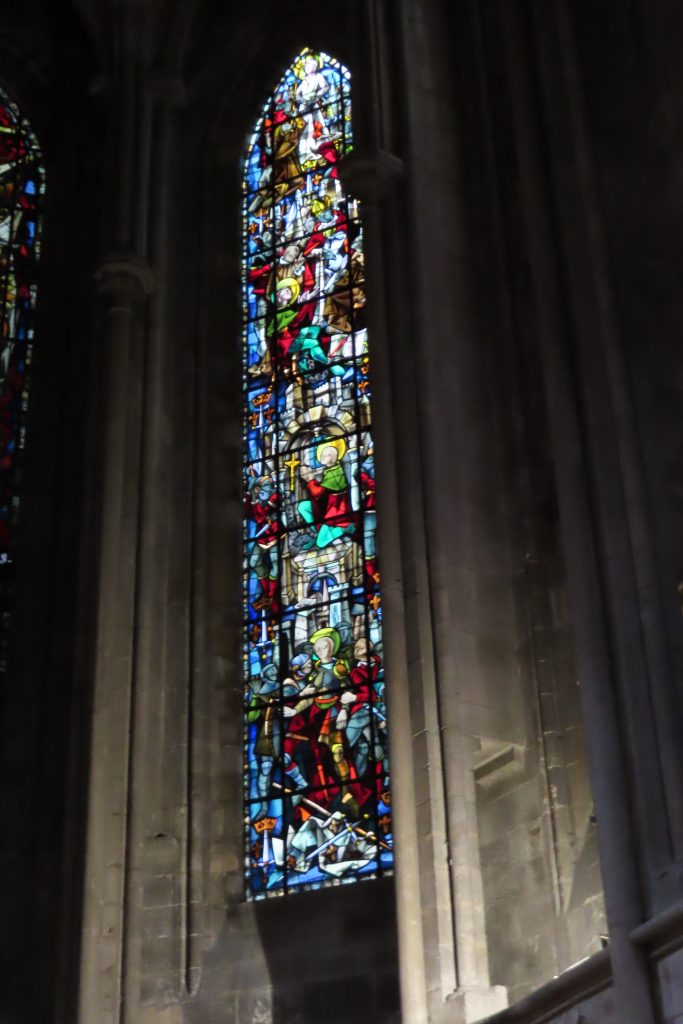
The day started with a walking tour of Rouen. We spent most of our time at the Rouen Cathedral – whose central spire is undergoing some renovation. Rouen is also notable because that is where Joan of Arc met her untimely death. The image below, after the statue, tells the tale in imagery.
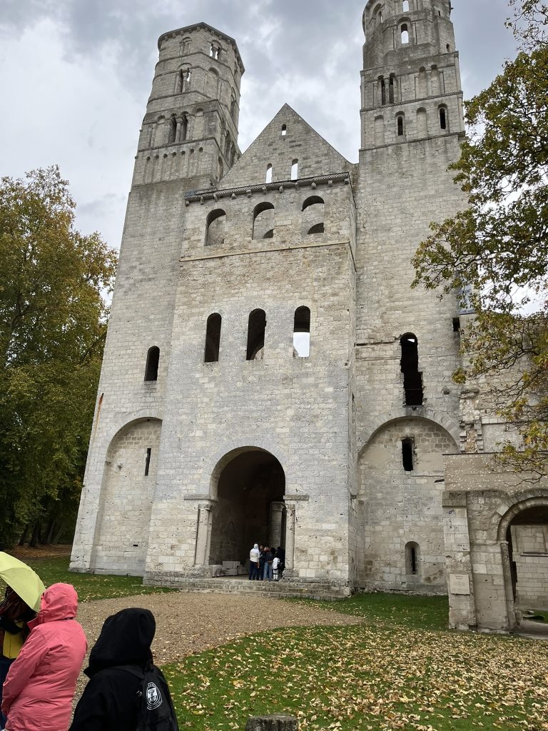
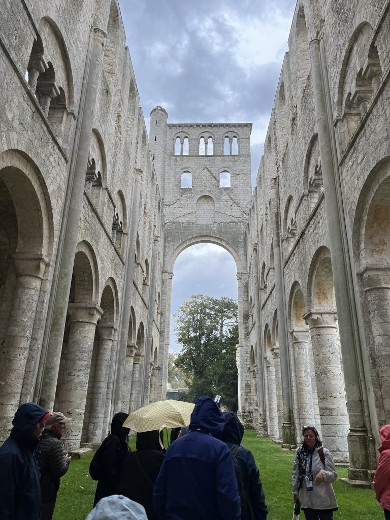
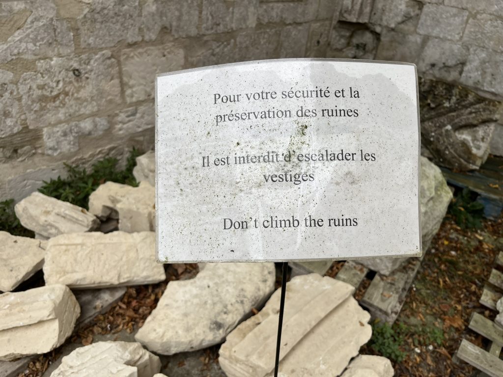
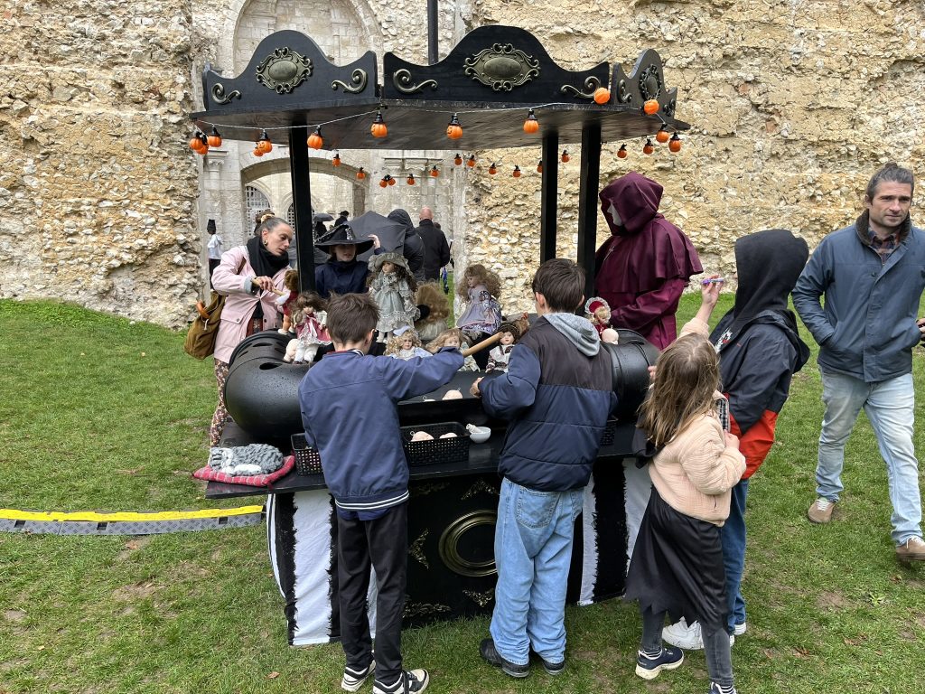
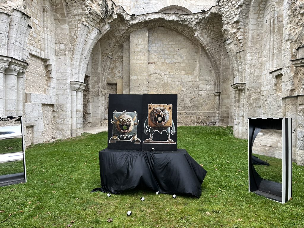
In the afternoon we took a bus to two abbeys in Normandy. The first one was Jumieges Abbey, and is in ruins, having been destroyed during the French Revolution. That day they were having a Halloween celebration of sorts.
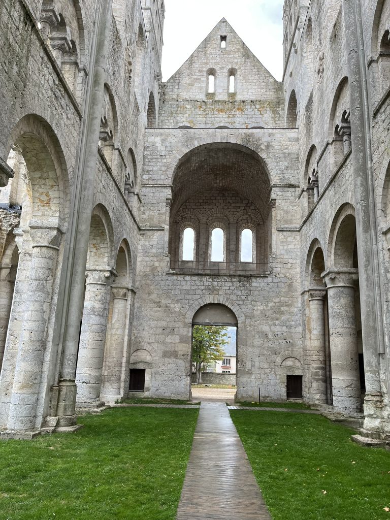
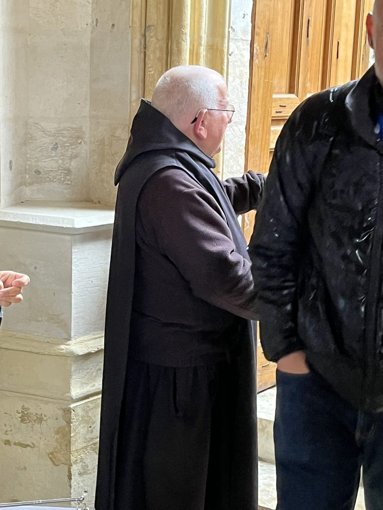
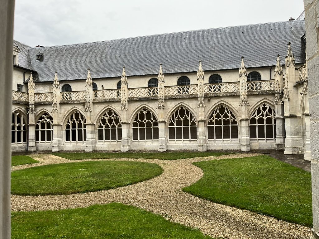
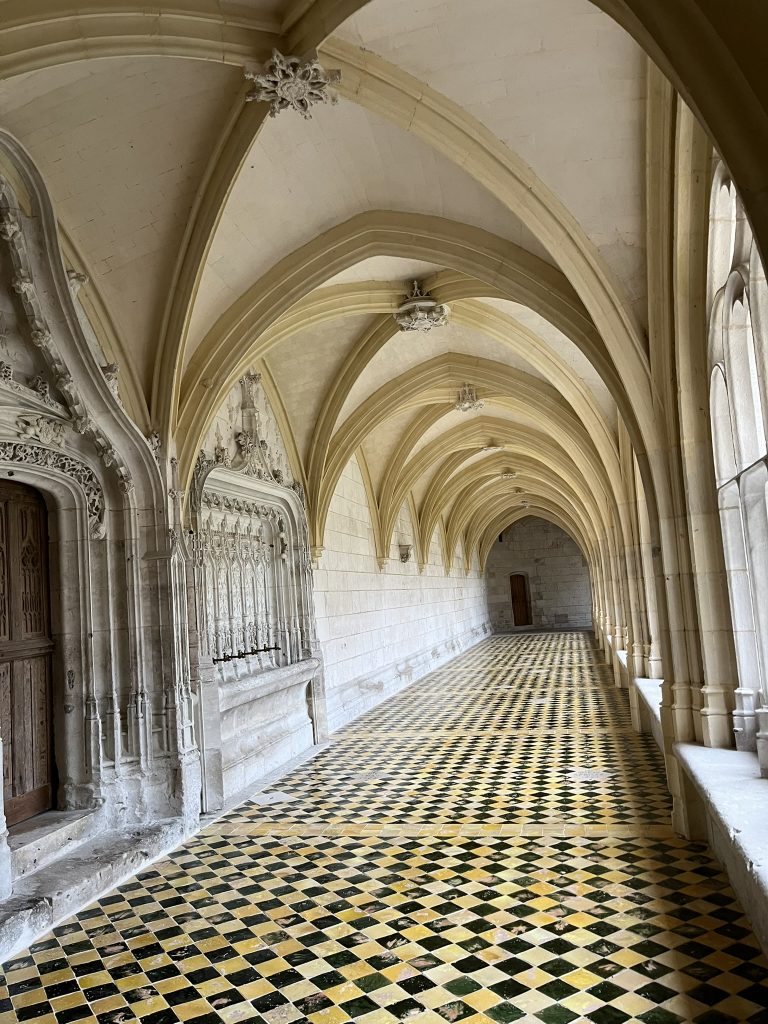
After Jumiges Abbey, we took the bus to Saint-Wandrille Abbey – which is still in operation. Restoration is being done on a continuous basis, from contributions (like I made) and also from sales at the gift shop — encouraged by the delightful monk who guided us on our tour through the abbey.
After returning to the ship, we continued on, sailing to Honfleur.
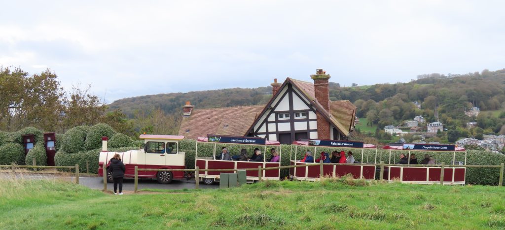
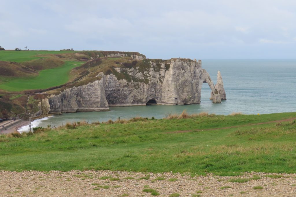
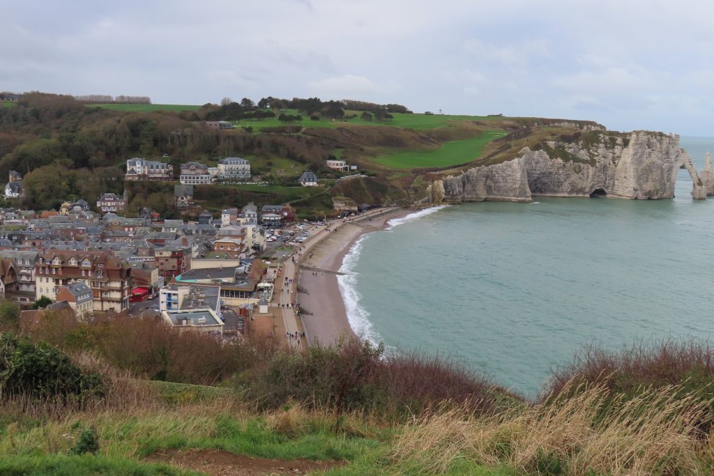
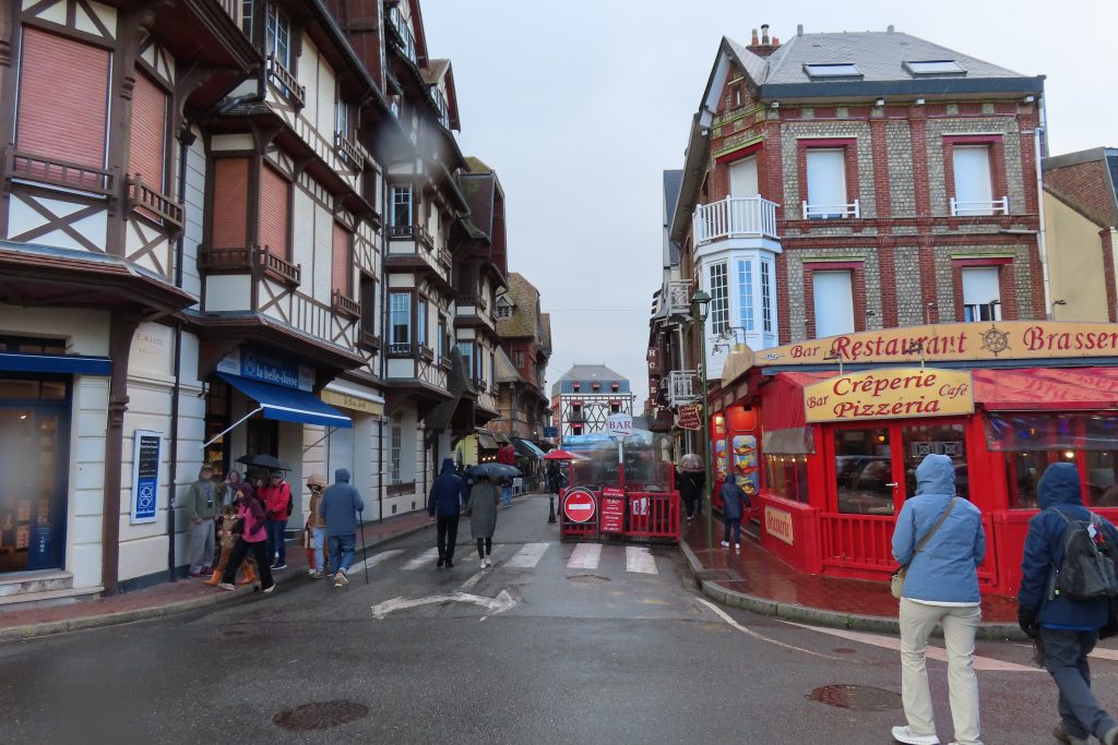
Day 7 – Honfleur and the cliffs of Etretat.
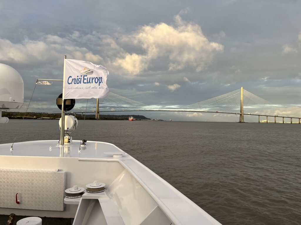
After sailing under the Pont de Normandie between Honfleur and Le Havre early in the morning, the next day’s excursions begain with a trip to Etretat, a delightful little town North of Le Havre. There we also visited the cliffs, consisting of limestone and darker flint, by way of a little open-air “train” of sorts.
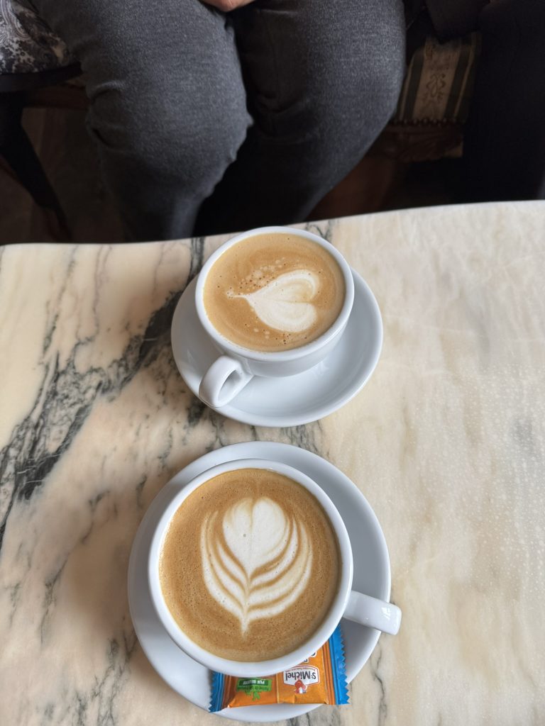
While I was wandering around Etretat, Gail and our new acquaintences Sam and Karen had some coffee at a cafe.
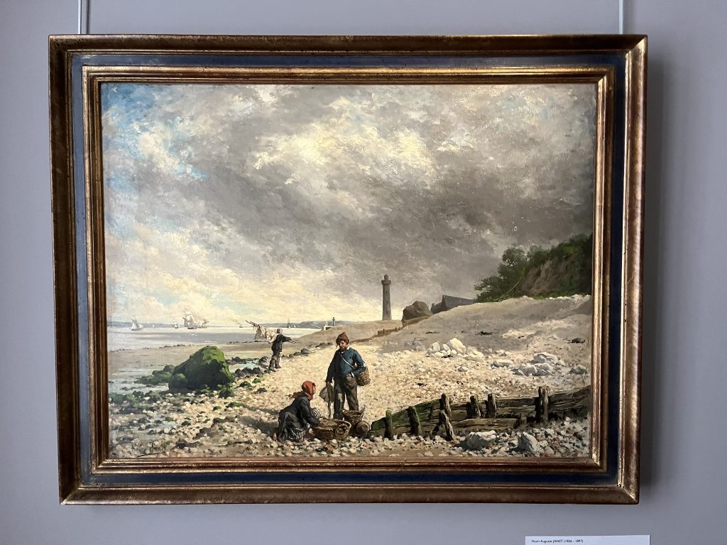
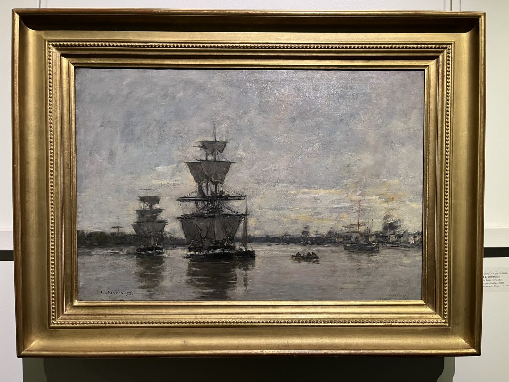
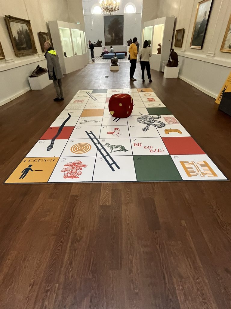
After lunch, we took a tour of the Eugene Boudin Museum. Boudin is said to have mentored and inspired Claude Monet in his work. I took lots of pictures of realistic paintings of ships and seascapes. We also saw a room-sized game of snakes and ladders.
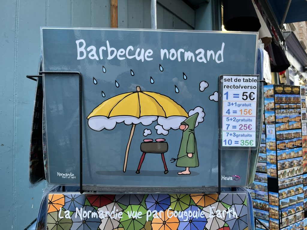
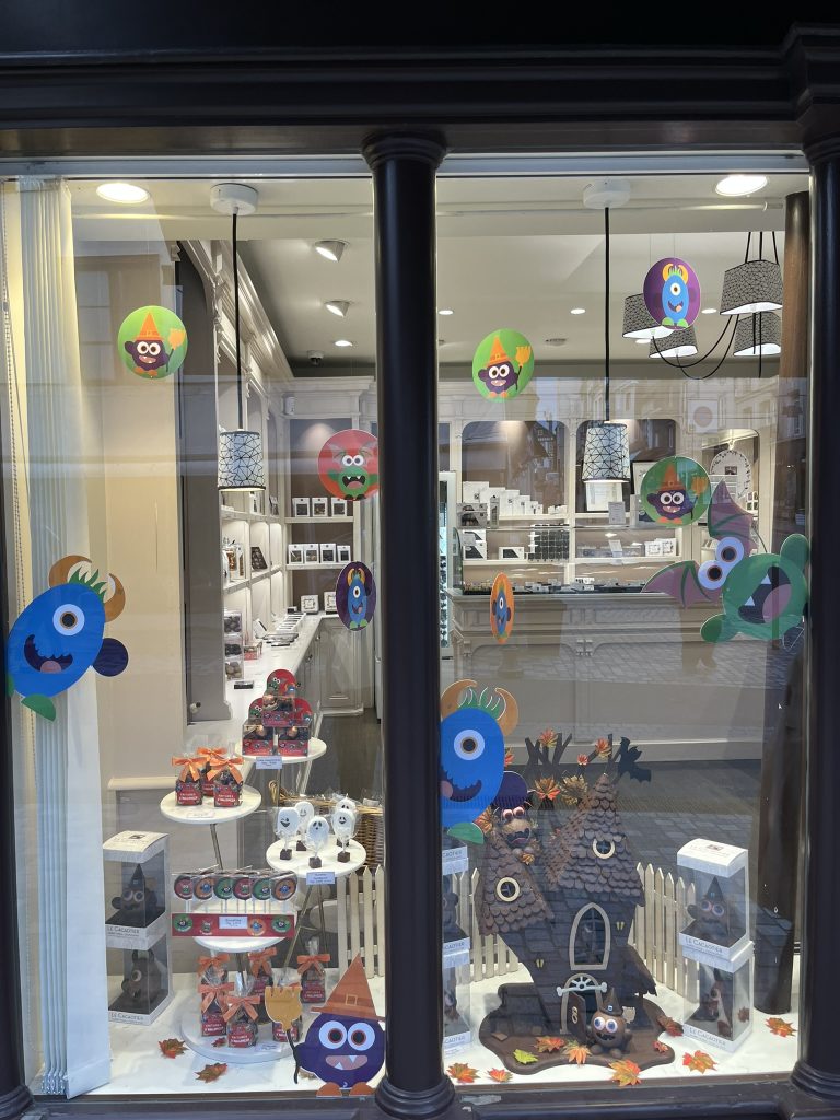
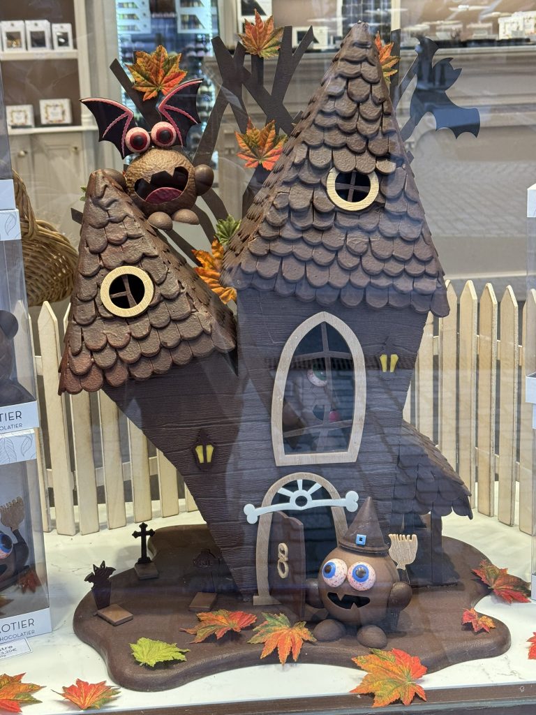
After the museum, Gail and I opted out of most of the walking tour of Honfleur, and visited a touristy gift shop and bought some funny placemates, and the Cacaotier chocolate shop.
Day 8 – The WW II Beaches of Normandy
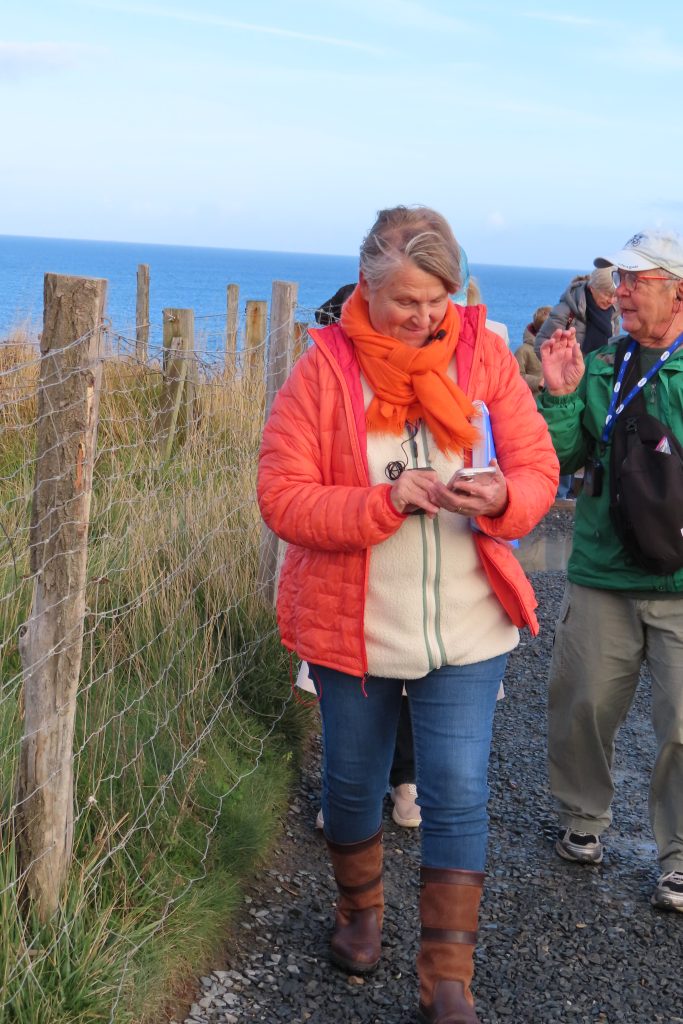
The beaches of Operation Overlord are legendary, of course, and with good reason. Such sacrifice! Our guide for the day was Marie – and a very wonderful guide she was – a Francophone for sure – but with a British accent to her English. She had all the facts and figures and stories one could want — all memorized, along with maps she could pull out when needed.
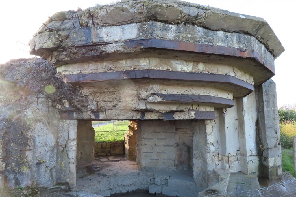
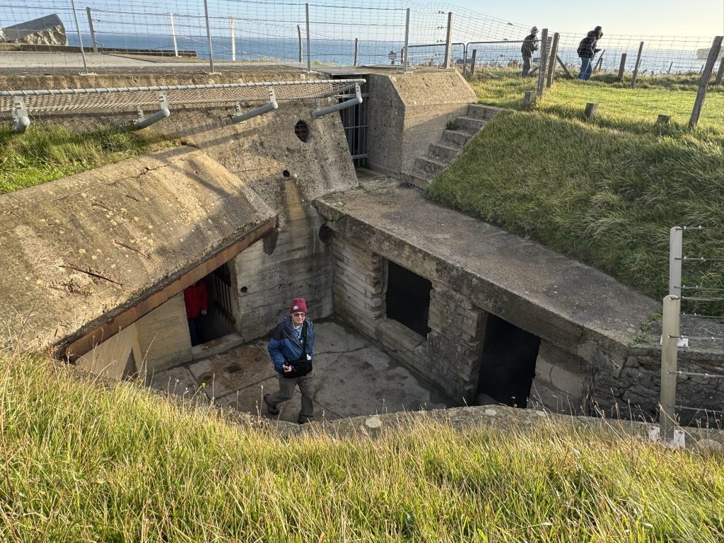
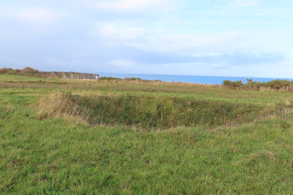
First we visited Pointe de Hoc, where U.S. Rangers scaled the cliffs, assigned to take out German artillery emplacements. However, it turned out that those guns, originally out in the open with no protection, had been moved, and telephone poles were in their place as decoy, and there were only German engineering troops there, buiding what they hoped would be protective bunkers for the guns when they returned (first photo, below). There was also a command post there (second photo), with bomb craters all over the place. Good thing there were fences to guide tourists!
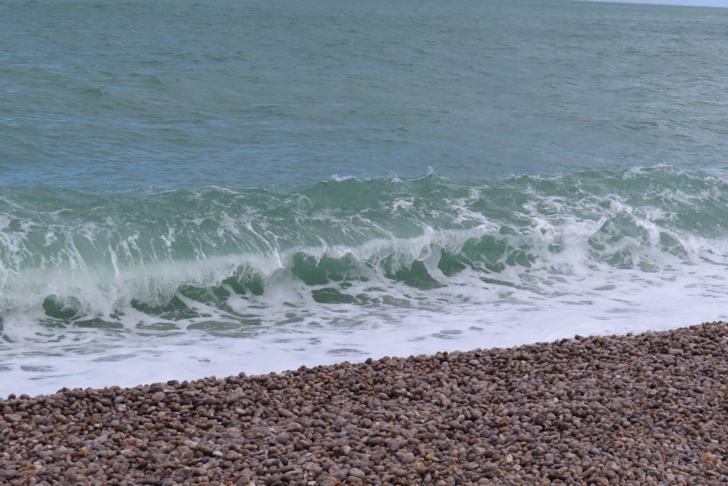
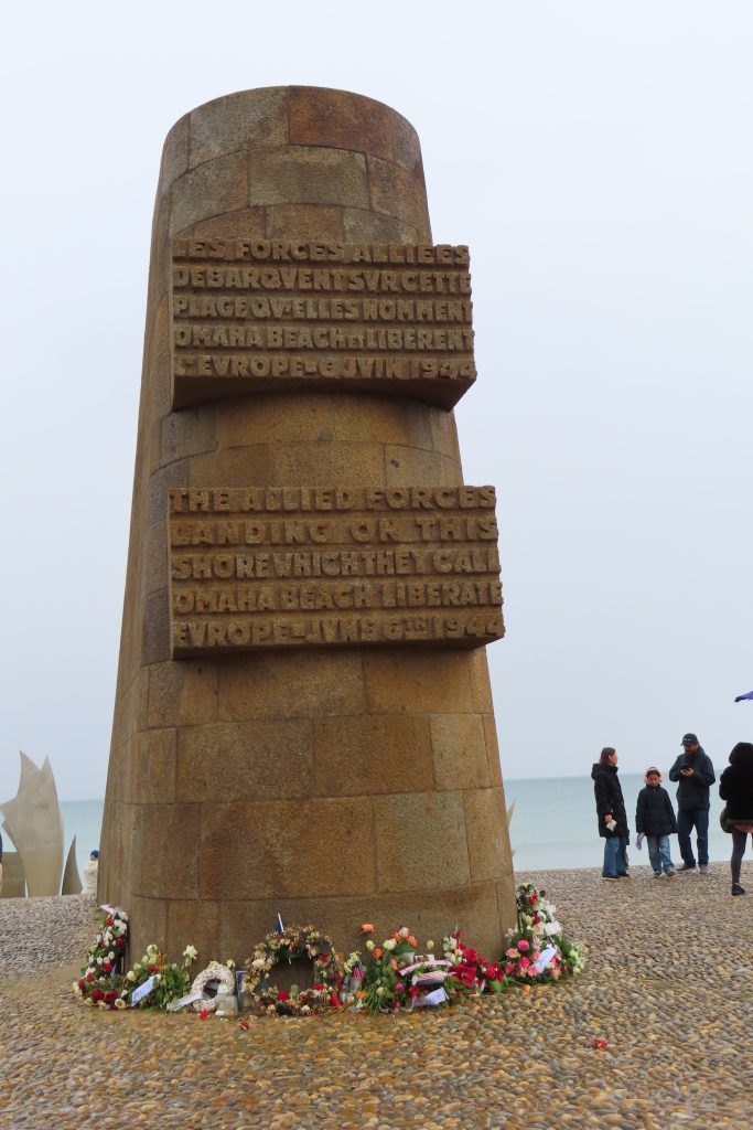
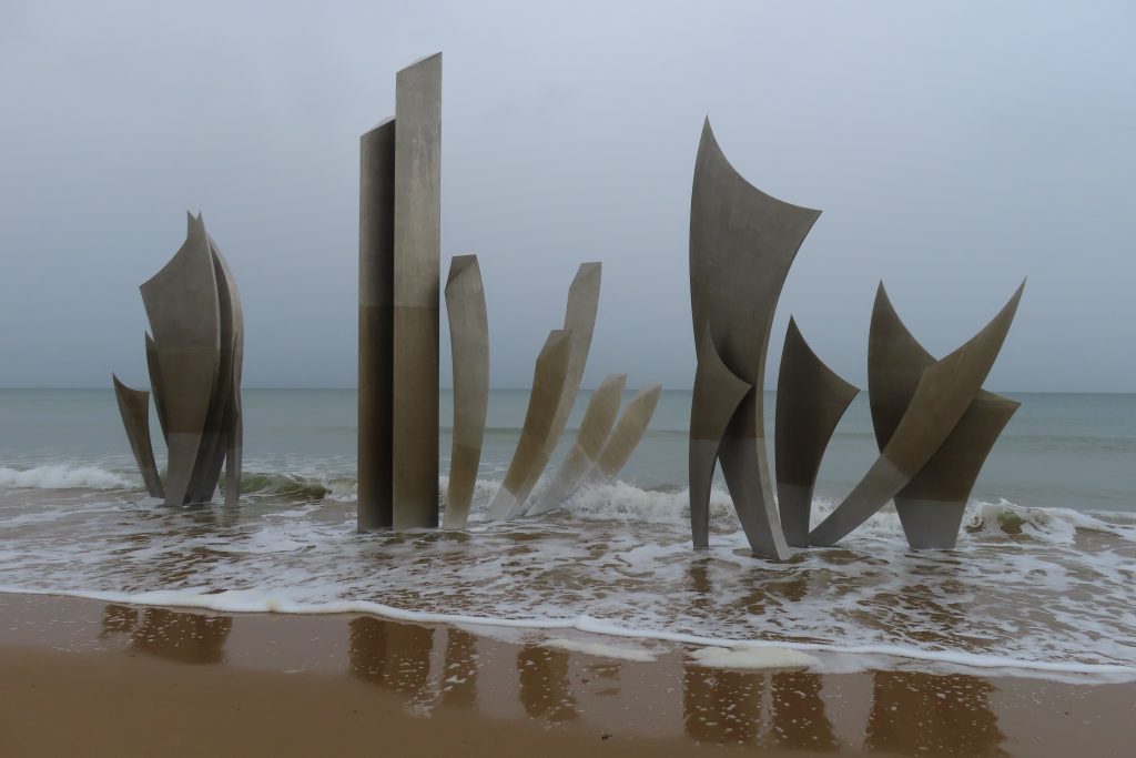
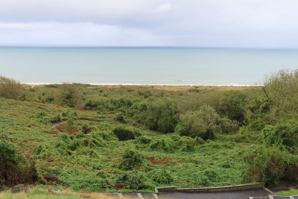
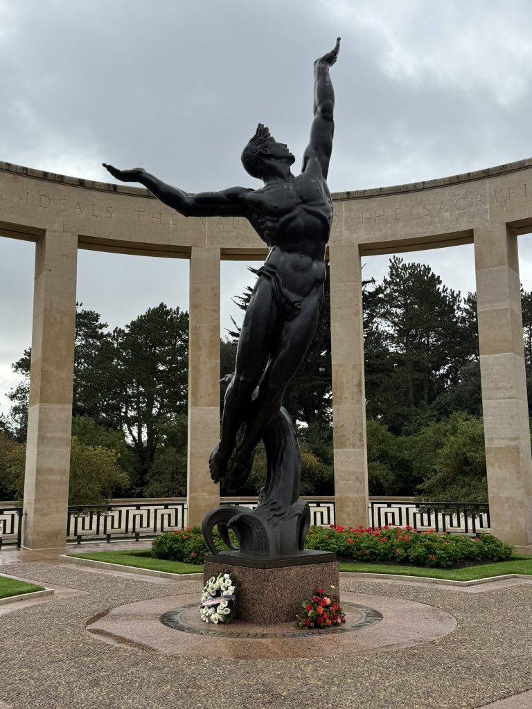
The next stop was Omaha beach, where so many of the American troops perished, and where I knelt down in the sand to pay my respects. (At the time of the invasion, the beach was not sand, but was instead pebbles, which caused any mis-aimed German fire to turn into shrapnel, multiplying the misery faced by the Americans. Thus, a lot of the monuments have pebbles surrounding them or inside their confines.) Below are the main monument and “Les Braves” sculpture.
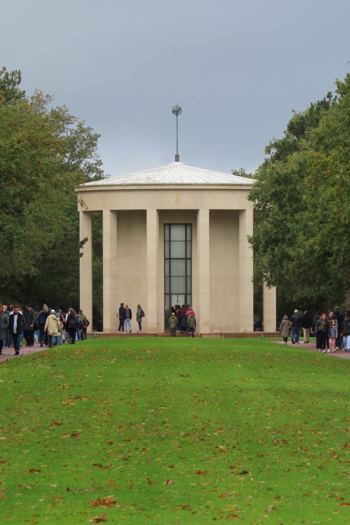
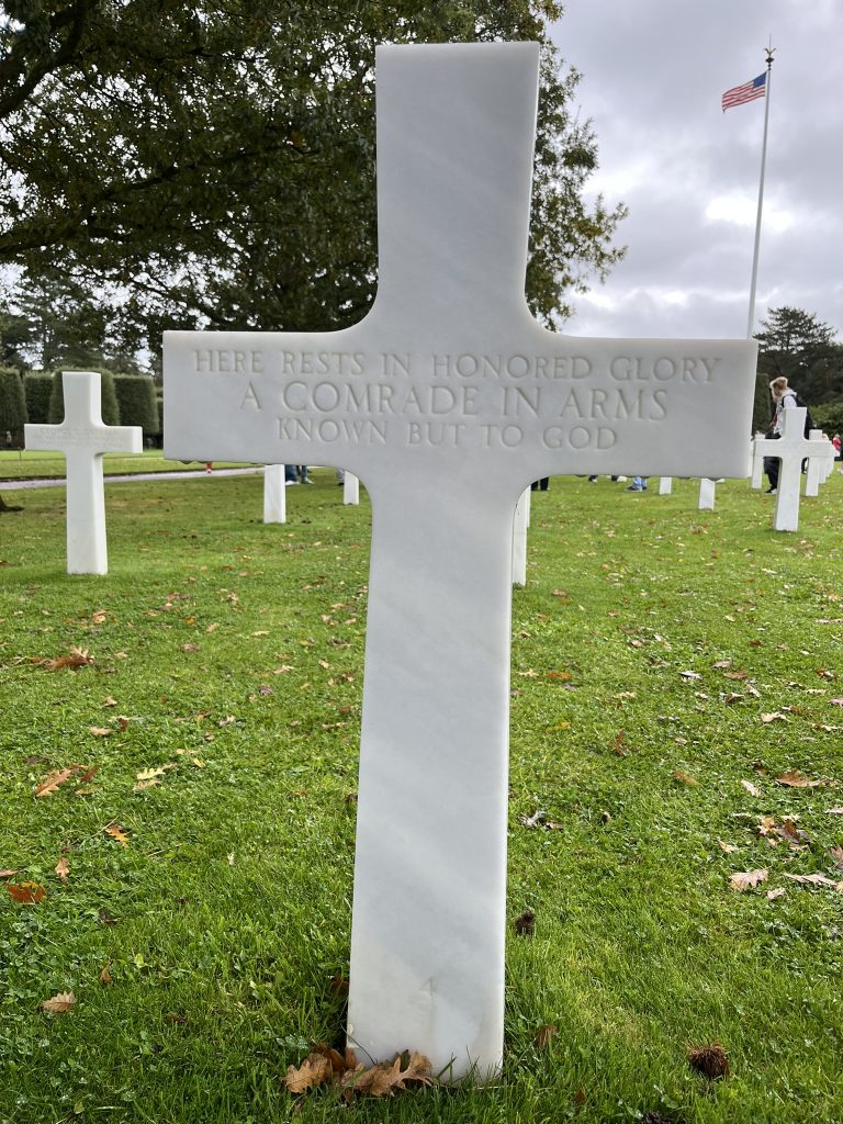
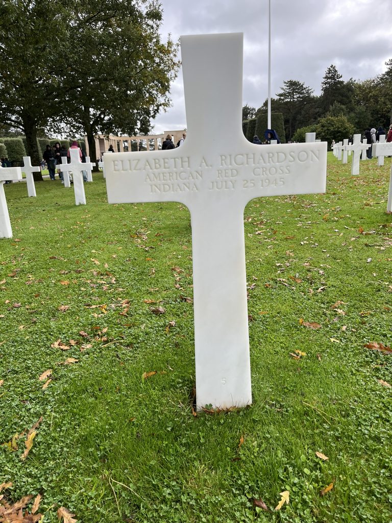
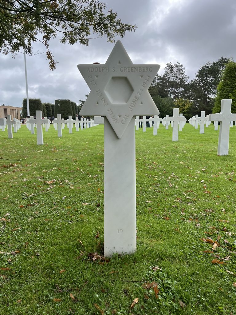
The last stop before lunch was Colleville-sur-Mer, the site of the Normandy American Military Cemetary, with its graves counting more than 9800, all aligned with great precision.
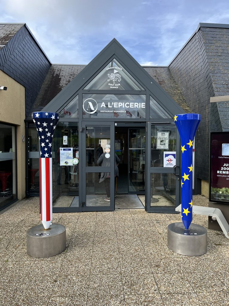
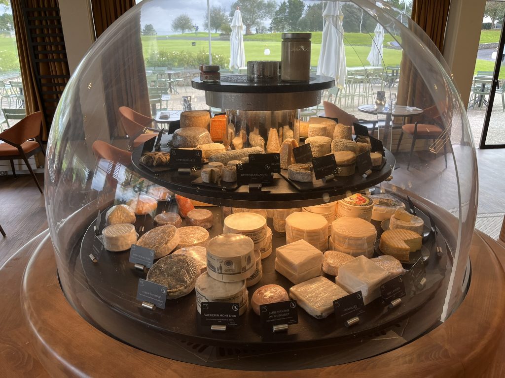
Then lunch – at a country club. (Yup, they golf in Normandy, in the rain.)
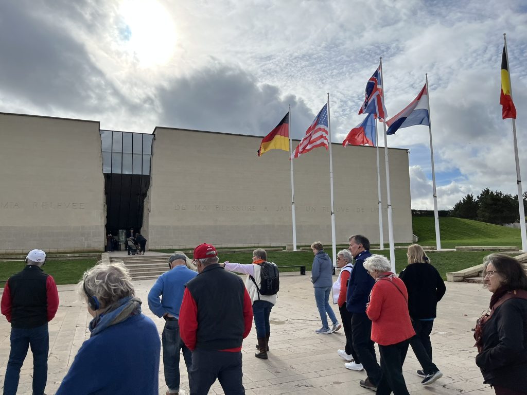
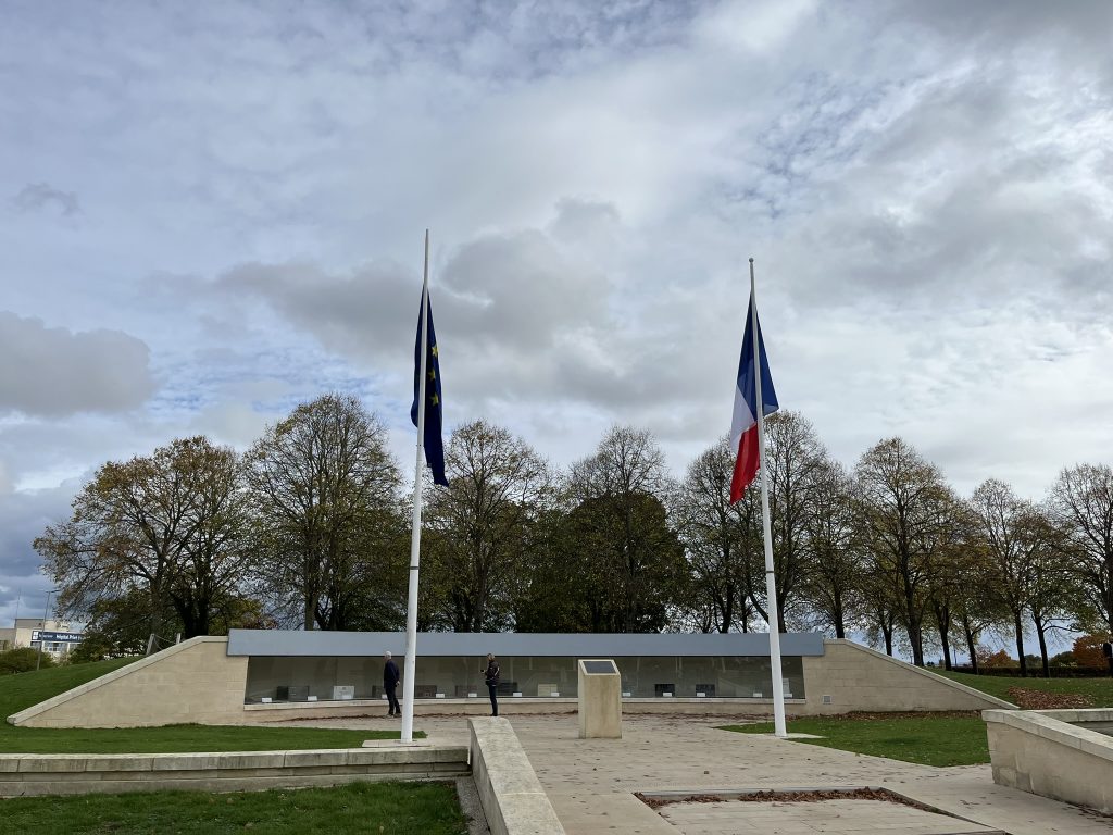
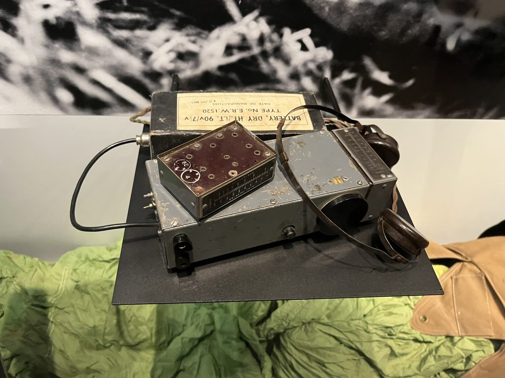
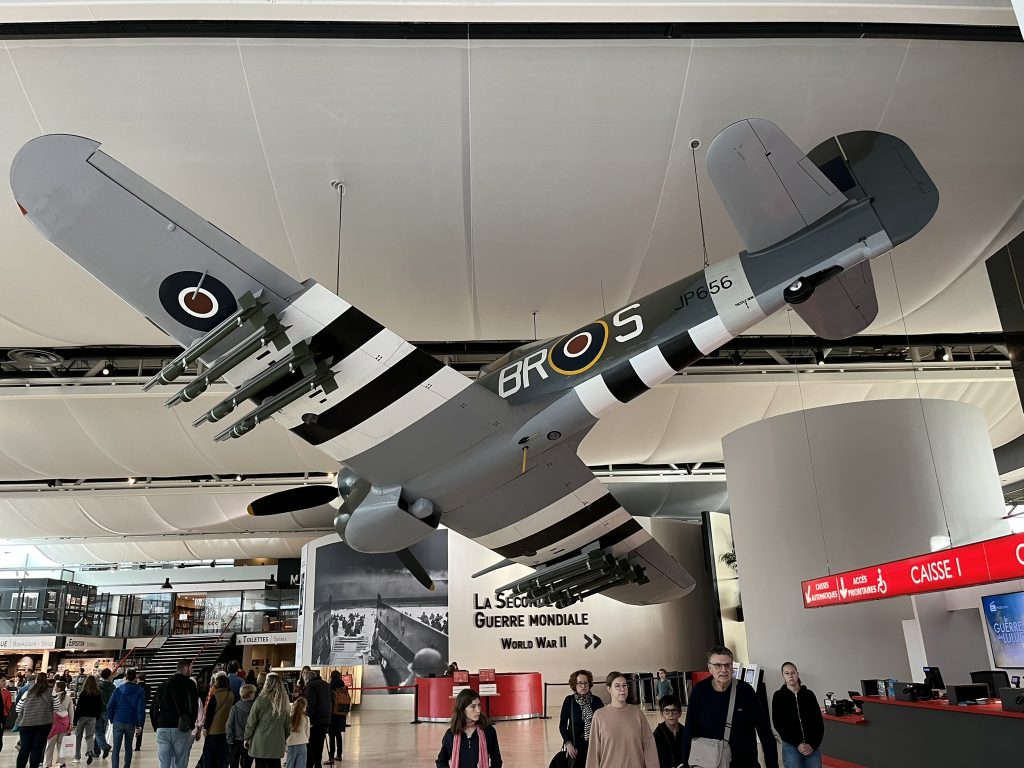
Following lunch, we paid a visit to the Caen Peace Memorial WW II museum.
Wow. What a day. On the way back I had a nice chat with tour director Rainer – but also felt my throat getting sore — as I was getting a cold (but fortunately *not* COVID).
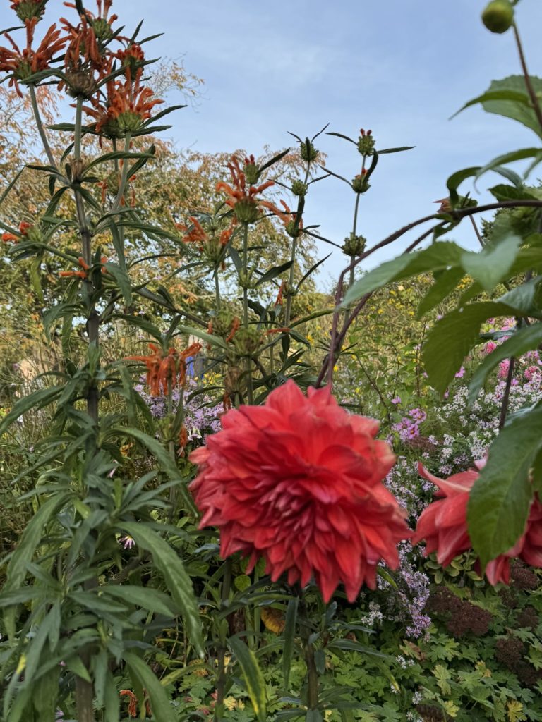
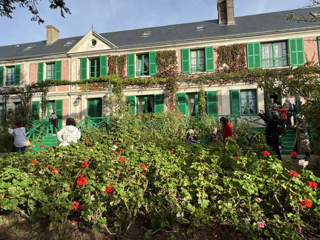
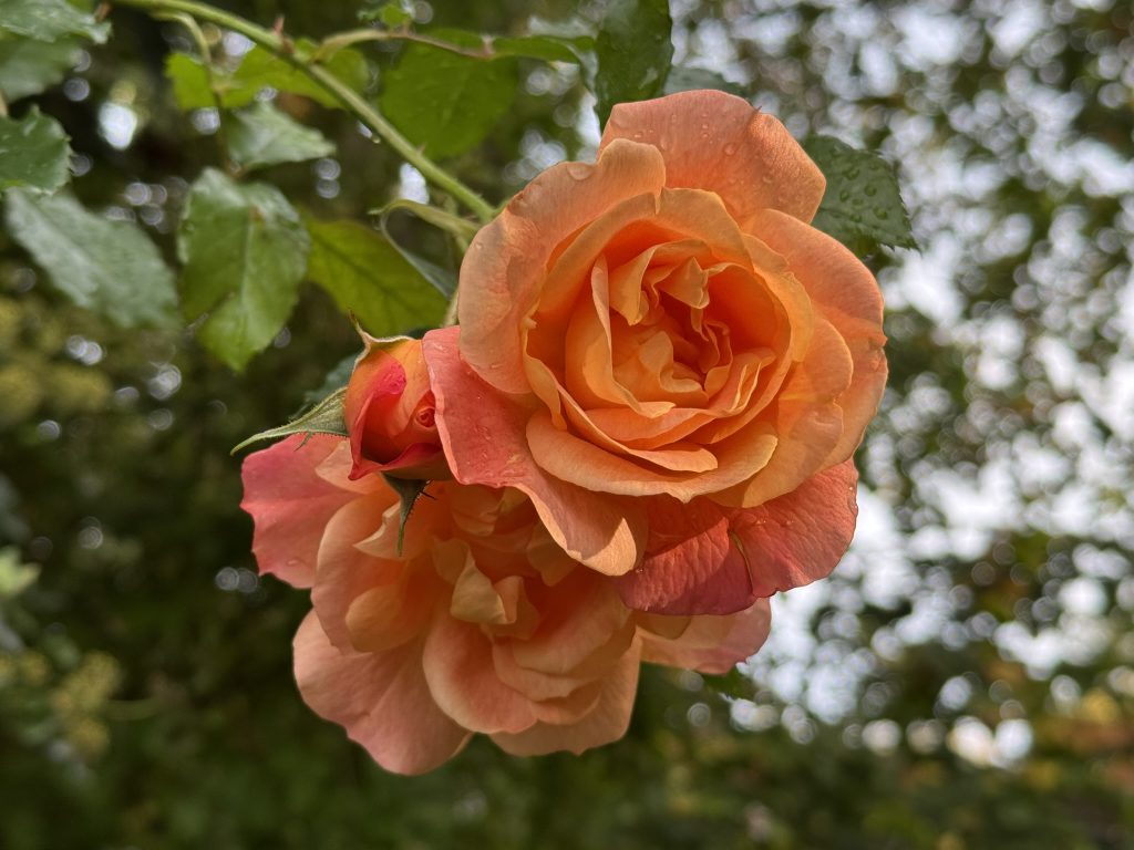
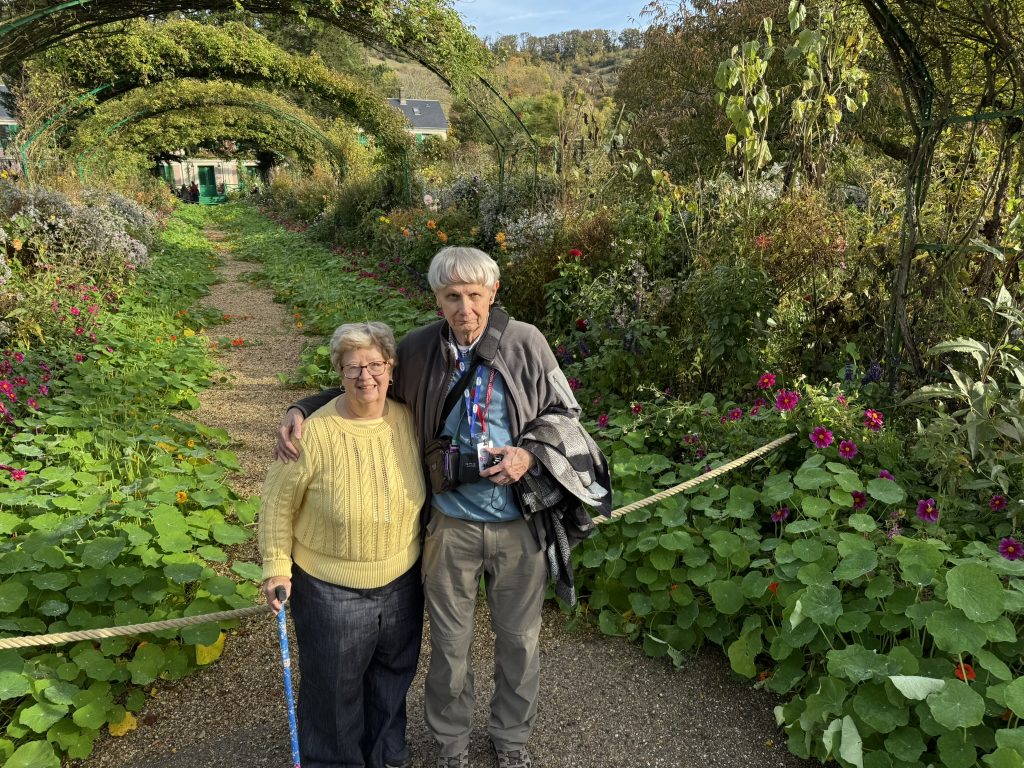
Day 9 – Claude Monet’s Home and Gardens
This was the last day we were really active on our trip (see Day 10) – a visit to Claude Monet’s home and gardens. We didn’t go into the home, but we explored the gardens thoroughly. Thanks to assistance from Fred and Rainer, we stayed behind the main group, but got early entry into the garden’s themselves.

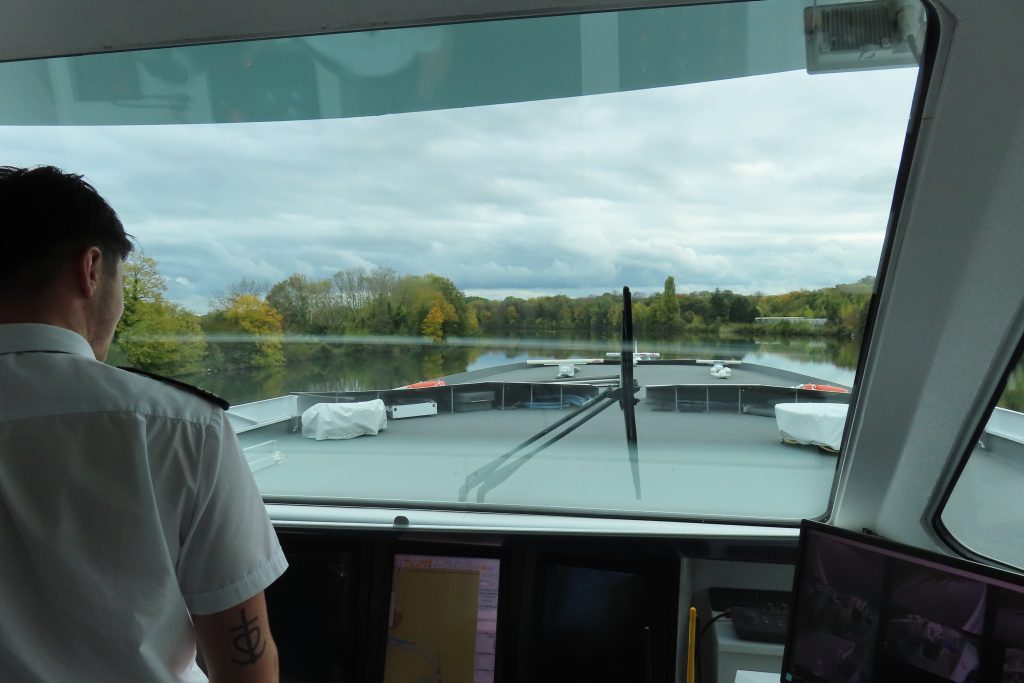
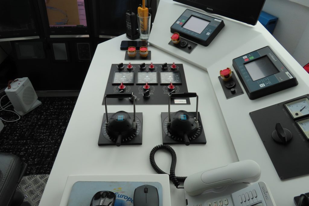
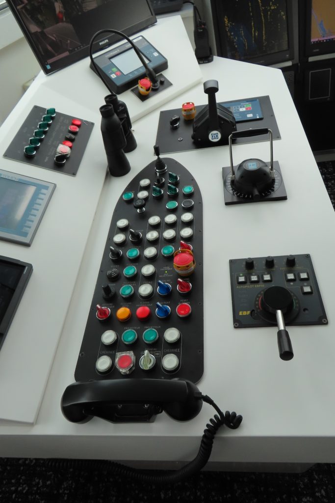
Later that afternoon, I had a chance to visit the ship’s wheelhouse.
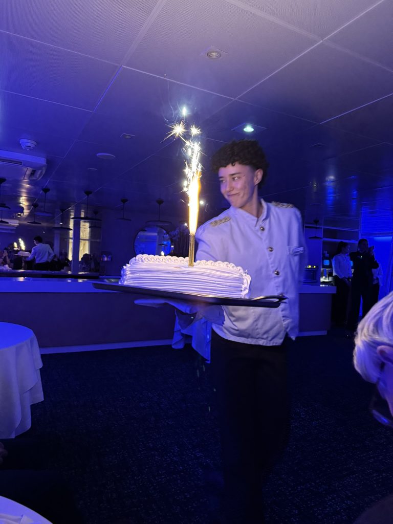
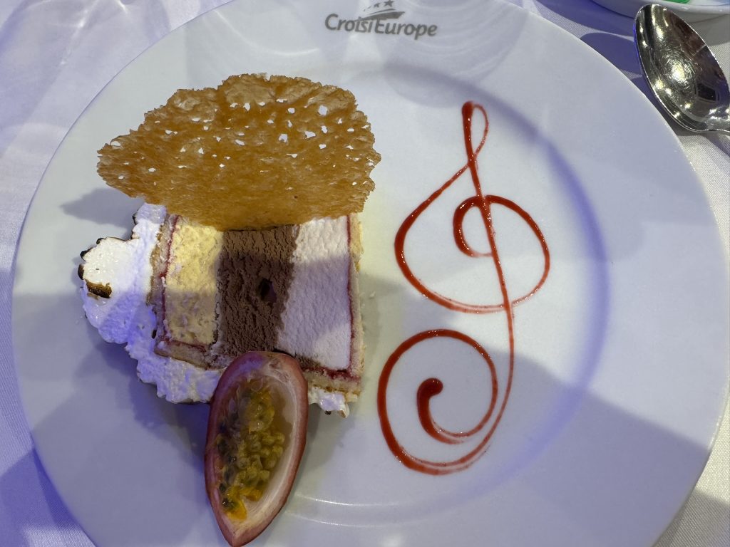
That evening’s event was the Gala dinner. It was held a day early because the next night was the night before we had to pack up and leave – with our bags to be ready at 5 AM. Dessert was baked Alaska, no less.
Day 10 – Back to Paris
Overnight the ship returned to Paris, to the same dock where we had joined the ship. The weather was windy and potentially rainy, and as we had already taken a bus tour of Paris, had sailed thru Paris at night, visited Notre Dame, and had walked around a couple of areas, we opted out of the river tour and walking tour of the Latin Quarter.
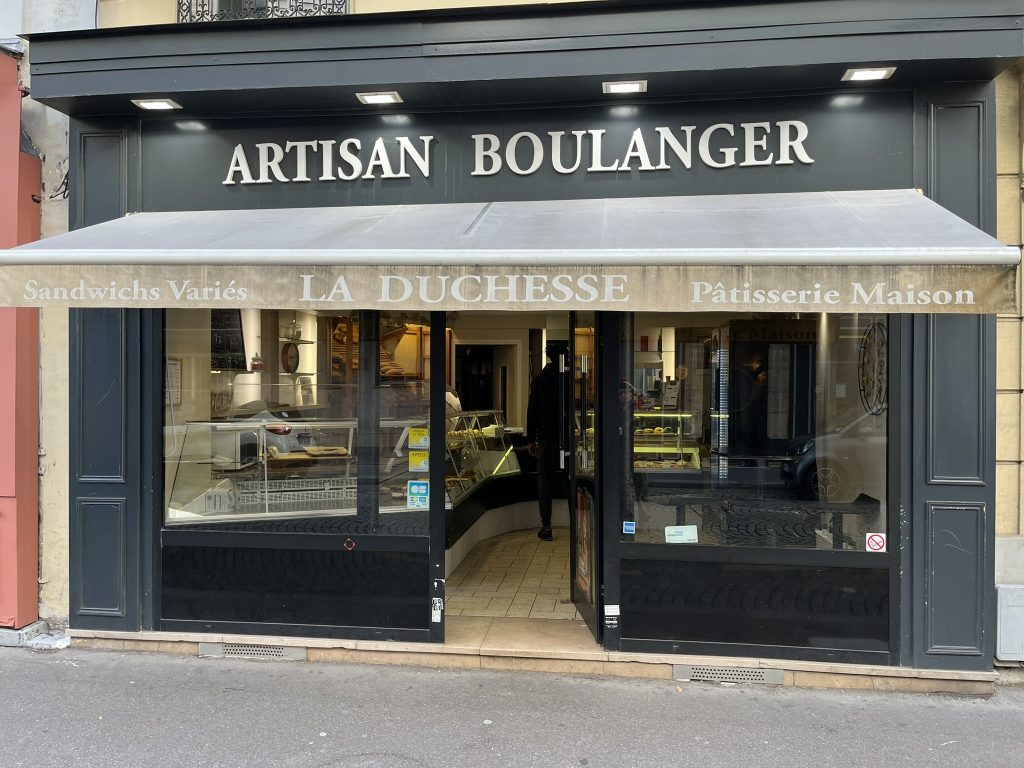
But I still had one item on my Paris “bucket list” — to visit une patisserie! Fortunately there was one just a few blocks from the dock — La Duchesse. Yum!
Day 11 – Back to Madison
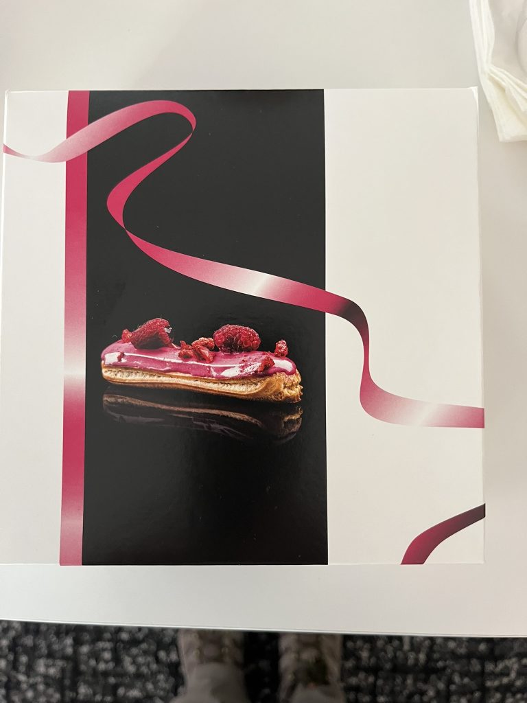
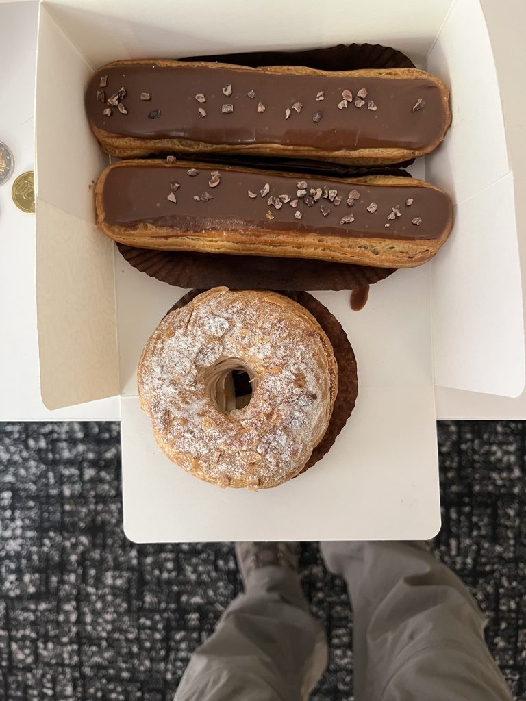
Waking up at 4AM, it was time to pack our bags before 5AM, and grab “un croissant” and some of the pastry I bought the day before, before boarding the bus at 5:30 for L’Aeorport Charles de Gaulle (CDG). The traffic was light, but the bus dopped us off at terminal 2F (we were told that was the closest it could get to terminal 2E), which meant a long walk to our terminal, which was tough for Gail. The AHI person handling our bags suggested we ask for mobility assistance, which we did.
The person assigned to Gail was a perhaps 30-something young woman, who as very nice, but spoke no English. She often asked how Gail and I (I was walking, carrying our carry on items) were doing (“Ca va?”) and took great care of us. We were escorted through border control and security. Just as we got to emmigration, the person in the booth we expected to visit went on break, and I could see that our escort was puzzled and annoyed by that some. After border control we then took a rather circuitous route down to the lowest level near a door to the tarmac. We were shuffled from chair to chair – it was a little disconcerting because we didn’t know how we were going to get from terminal 2K, where we were, to 2M. Our escort finally resorted to Google translate (or some such) to let us know a bus (a van, actually) would pick us up. The van then dropped us off at terminal 2E M – where our gate was. We chose to walk to the gate as we had plenty of time. Fortunately, just before bording our escort reappeared with another customer, and I was able to slip her a small tip, for which she seemed greatful.
The service was very nice but the initial wait for our escort was more than 15 minutes, as was the wait for the van, so our whole experience was nearly two hours, whereas when we arrived and navigated through things ourselves we got through in maybe 75 minutes.
The flight home was uneventful. Getting through Detroit DTW involved some walking which was a little tough for Gail, but straight-forward. The immigration officer seemed to be doing double duty as customs, as he also asked what we had returned with (and I also had used the handy MPC app to make our declarations). Retriving my Apple watch from the TSA agent (see above), we then snagged our luggage off the carousel and took it to the special connecting flight check in spot – a nice arrangement. We were a little concerned because the bar code on Gail’s bag had been completely mangled, folding over itself, but both of our bags made it onto the plane and showed up in Madison.