
With the 1410 mode CPU running correctly, it was time to test out the 1401 side of things. The 1410 has a toggle switch, allowing the CPU to run as an IBM 1401 compatible with most 1401 programs. The 1410 and 1401 are similar, architecturally. The biggest difference is that the 1401 uses 3 character addresses, with the zone bits over the units and hundreds positions in order to address up to 16,000 characters, whereas the 1410 uses 4 character addresses, capable of addressing memory up to 100,000 characters.
The primary 1401 diagnostic is M011. Once I figured out a problem involving the 1401 addressing scheme, I turned my attention to the next failure: The Store A Address Register (SAR) instruction died a horrible death with B Channel, Address Channel and B Character Select Errors. That problem manifested as a failure to copy the A Address Register to the B Address Register for storing later. I tried for a bit to fix this first, but was not immediately successful, so I decided to try and NOP out the uses of SAR, that mostly had to do with storing the address of each test so it could print out a failure message.
Having done so, the next problem quickly cropped up: the partner instruction for the B address register, Store B Address Register (SBR) also failed – it is essentially the same as SAR, but without that first step of transferring the AAR to the BAR. And the failure error was different as well: an Address Chanel Exit error. The ALD for this circuit is 18.14.02.1 . The ILD is on figure 59 at coordinate 2B – however there is also an error in that ILD. It shows the GateOff input to trigger DEZ as ground (the usual ground symbol). However, on the ALD, the F input it connect to M, which is -12 Volts, and in my scheme, that is logic 0. (Logic 1 being 0V).
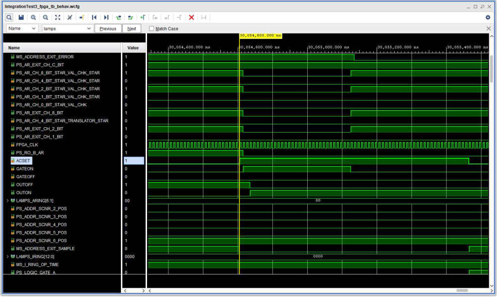
The timing diagram below shows the timing issue. The B Address Register read out and validity check look like they are OK with respect to the Address Exit flip flop ACSET signal. However, the problem was that the VHDL for implementing the SMS card type DEZ has a 3 clock cycle “silo” for ACSET, so that the flip flop is not really set until 3 clock cycles after its ACSET input. In addition, there was no such silo for the other inputs. This silo was put in place to give the ACSET signal some noise immunity – so that a 1 cycle glitch would not set the trigger. But the fact that the other inputs did not have a silo meant that they were sampled 3 clock cycles (FPGA_CLK) after ACSET, and by that time the B Address Register Readout signal (PS_RO_B_AR, i.e. +S RO B AR) had become inactive.
The relevant VHDL looked like this:
   SMS_DEZ_PROCESS: process(FPGA_CLK, ACSET, DCSET, DCRESET, DCRFORCE, DCSFORCE)
        begin
        if(rising_edge(FPGA_CLK)) then
           if(DCRESET = '0' OR DCRFORCE = '1') then
              OUTOFF <= '1';
              OUTON <= '0';
              SSTAGE1 <= ACSET;
              SSTAGE2 <= ACSET;
              SSTAGE3 <= ACSET;
           elsif(DCSET = '0' OR DCSFORCE = '1') then
              OUTON <= '1';
              OUTOFF <= '0';
              SSTAGE1 <= ACSET;
              SSTAGE2 <= ACSET;
              SSTAGE3 <= ACSET;
           else
              SSTAGE1 <= ACSET;
              SSTAGE2 <= SSTAGE1;
              SSTAGE3 <= SSTAGE2;
              if(GATEON = '1' AND SSTAGE2 = '1' AND
                SSTAGE1 = '1' AND SSTAGE3 = '0') then
                  OUTON <= '1';
                  OUTOFF <= '0';
                elsif(GATEOFF = '1' AND SSTAGE2 = '1' AND
                  SSTAGE1 = '1' AND SSTAGE3 = '0') then
                   OUTOFF <= '1';
                   OUTON <= '0';
               end if;
            end if;
        end if;
        end process;
Once I realized what was going on, the fix was pretty easy. Just add a 3 clock silo for the inputs as well as ACSET. I took the conservative approach, however, and created a separate special instance of SMS_DEZ.vhdl, called SMS_DEZ_SYNC.vhdl to use in the Address Exit validity check logic. This new implementation of DEZ would probably work fine across the board, but I am just using it in the one place, for now.
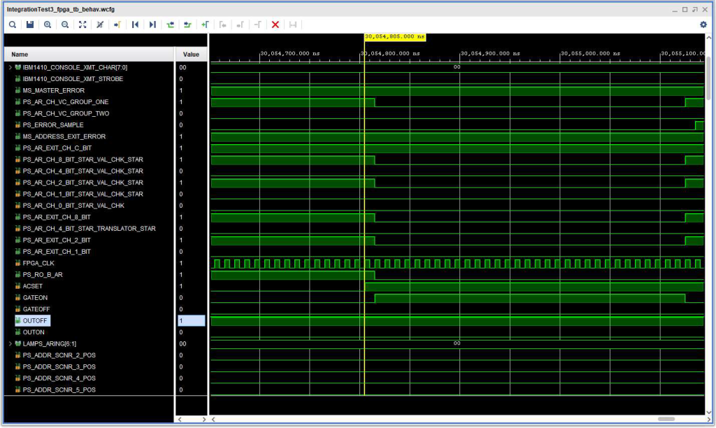
The timing diagram below shows that now the OUTON signal does not activate – no Address Exit Check, because now the inputs are sampled at the same time as ACSET, and those inputs are still active from the B Address Register readout.
The relevant VHDL looks like this, for gate type SMS_DEZ_SYNC:
    SMS_DEZ_PROCESS: process(FPGA_CLK, ACSET, DCSET, DCRESET, DCRFORCE, DCSFORCE)
        begin
        if(rising_edge(FPGA_CLK)) then
           if(DCRESET = '0' OR DCRFORCE = '1') then
              OUTOFF <= '1';
              OUTON <= '0';
              SSTAGE1 <= ACSET;
              SSTAGE2 <= ACSET;
              SSTAGE3 <= ACSET;
              GON1 <= GATEON;
              GON2 <= GATEON;
              GON3 <= GATEON;
              GOFF1 <= GATEOFF;
              GOFF2 <= GATEOFF;
              GOFF3 <= GATEOFF;
           elsif(DCSET = '0' OR DCSFORCE = '1') then
              OUTON <= '1';
              OUTOFF <= '0';
              SSTAGE1 <= ACSET;
              SSTAGE2 <= ACSET;
              SSTAGE3 <= ACSET;
              GON1 <= GATEON;
              GON2 <= GATEON;
              GON3 <= GATEON;
              GOFF1 <= GATEOFF;
              GOFF2 <= GATEOFF;
              GOFF3 <= GATEOFF;
           else
              SSTAGE1 <= ACSET;
              SSTAGE2 <= SSTAGE1;
              SSTAGE3 <= SSTAGE2;
              GON1 <= GATEON;
              GON2 <= GON1;
              GON3 <= GON2;
              GOFF1 <= GATEOFF;
              GOFF2 <= GOFF1;
              GOFF3 <= GOFF2;
              if(GON3 = '1' AND GON2 = '1' AND GON1 = '1' AND GATEON = '1' AND
                SSTAGE2 = '1' AND  SSTAGE1 = '1' AND SSTAGE3 = '0') then
                  OUTON <= '1';
                  OUTOFF <= '0';
                elsif(GOFF3 = '1' AND GOFF2 = '1' AND GOFF1 = '1' and GATEOFF = '1' AND
                  SSTAGE2 = '1' AND SSTAGE1 = '1' AND SSTAGE3 = '0') then
                   OUTOFF <= '1';
                   OUTON <= '0';
               end if;
            end if;
        end if;
        end process;
With that out of the way, I could run M011 diagnostics quite far into the tests, until it needed to use the SAR instruction for more than just tracking the test address.