Came across something interesting today on Automatic Logic Diagram 13.50.04.1. It refers to unit “8” – which is for punch column binary – a special feature. An 8 character is just the 8 bit – odd parity. However, to decode unit 8 per the ALD one would have to have B 8 – and no check bit – even parity- which can never happen. So, if one were going to have the column binary feature installed, it would require an actual rework to change the input to one of the pins on ALD 13.50.04.1, coordinate 3A (11DJ02) from “+S E CH U SEL REG B BIT” to “+S E CH U SEL REG NOT B BIT”. So, without this rework, the machine would simply not decode unit 8 at all – perhaps intentionally. (Of course, on the generated version, this would be an easy fix, but for now I just left it as is.)
Month: July 2020
IBM 1410 ALD to FPGA – I “got one”
I have been testing the logic generated from each Automated Logic Diagram (ALD) page, using the Instructional Logic Diagrams (ILD) were available to guide my testing. Until today I don’t recall finding any cases where I actually made a connection mistake when I entered the ALDs into the database – until today. On page 13.50.01.1, I had mis-substituted signal “-S I-O Lozenge Latch” where I should have had “+S Logic Gate E 1” as the input to the gate at coordinate 5H. The testing caught it.
When I entered data for each sheet, I tracked usage of each signal count. I had a “2” written next to “+S Logic Gate E1” — as I should have. I must have missed that when I checked the signal usage counts after entry (“-S I-O Lozenge Latch” had the two instead). The latter is right below the former on the left side of the ALD, which made the mistake not unlikely, and made it easier to mis-interpret where I had written the signal count of 2. I even circled the 2, meaning I checked it. Oops.
Finally, a Radio Antenna
Over the past couple of months I have been working planning, and now, this last week, installing a radio antenna suitable for Ham frequencies (in particular, 10, 20 and 40 meter wavelengths).
The antenna installation comprises:
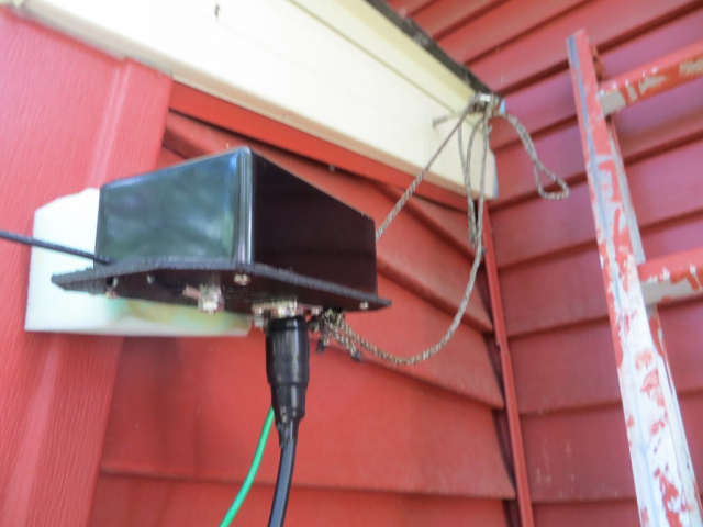
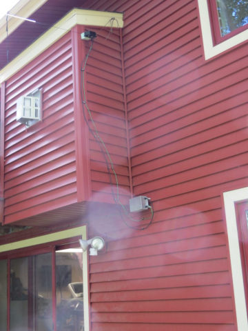
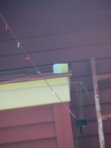
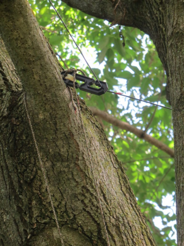
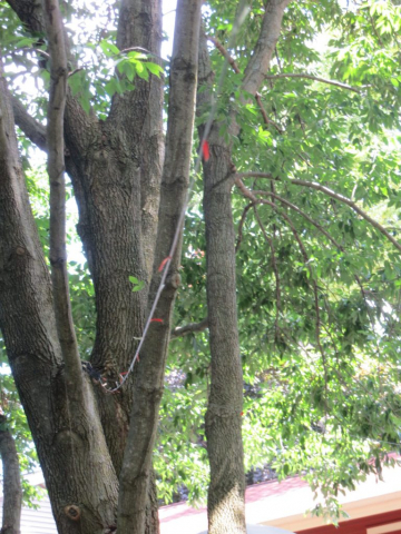
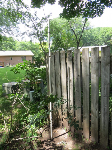
- A 60′ plus antenna wire, run from our cut-off chimney, then passes though a tree supported from a limb, and then is attached via a rope to a 10 foot high PVC pipe which is sunk into the ground 2 feet, which provides support for the far end (and keeps it well above my head.)
- An antenna matching transformer that matches the relatively high impedance of this “end fed dipole” antenna to the 50 ohm impedance of the coax feed line attached to it.
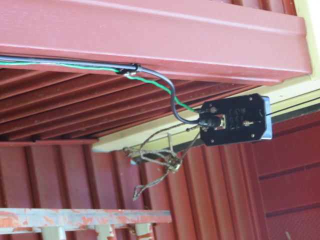
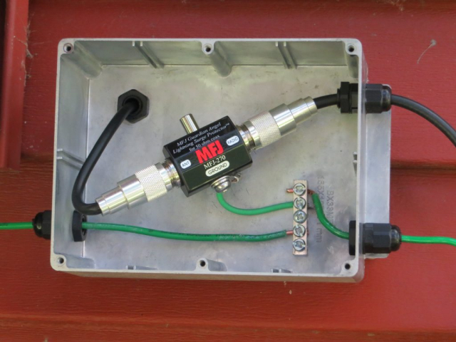
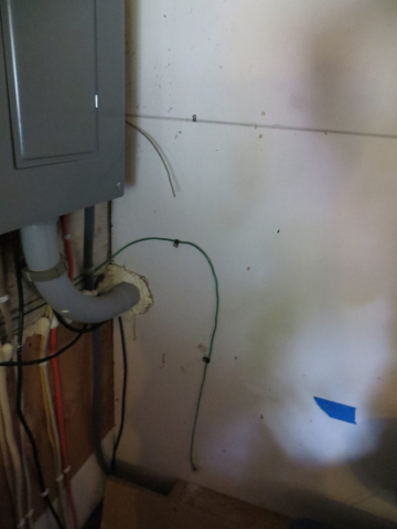
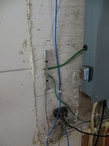
- A safety ground the leads down from the box containing the antenna matching transformer, to a metal box which connects this to the lighting arrestor ground and a ground that runs off to the inter-system ground (see below.)
- A lightning arrestor which is installed into the feed line, and which connects to the feed line into the house.
A big difficulty with my antenna installation was grounding. An antenna must have a ground, both to “work”, but also to provide static discharge to discourage lightning strikes.
If lighting strikes a typical antenna, it will vaporize and likely damage any equipment attached to it – that is not what the safety ground is designed to prevent. Rather, it attempts to discharge pre-lightning voltage build-ups.
An ideal ground is directly below the antenna, with a 6 foot or so rod driven into the soil. However, if that is done, it is also crucially important to “bond” that ground rod with any others on the property (such as one installed by the electric company.) The reason this is so important is that if lighting strikes the utility lines, it wants to find its way to ground, and will happily do that through your house wiring to find your radio ground, if the two ground rods are not bonded. The reverse is also true if lighting strikes the antenna.
However, in my case that would have meant running the AWG 6 (!!) bonding wire through a rock wall, which was rather impractical. So, instead, I opted to run the safety ground above ground, mounted under the deck, and connect up to the inter-system ground that was installed at my electrical panel in 2017 when that panel was replaced. That connection then connects it to the utility ground rod.
Here are some photos:
Note that the antenna box in the first picture, which contains the matching transformer, attaches to the eye bolt on the chimney with two lines of different lengths. Do you know WHY the lengths are different??? Leave a comment, below.
IBM 1410 ALD / FPGA Progress Report: Volume III Complete
I continue to make progress testing the logic generation from ALDs into VHDL. I have now completed the generation and testing of pages in Volume III, which includes the operation and operation modifier registers and decode.
To aid testing, I created a BCD enumeration, which, because VHDL enumerates them in order, starting at 0, made BCD character (by name, such as BCD_A) to binary string conversion easy, which facilitated testing.
I continue to find very few errors. I did find a couple of signal names with (consistent) typos and a few cases where gates had an input shorted to ground (logic 1 for SDRTL) where I removed that connection as handling it would have required code changes to the generation code which I did not care to make.
Q: When is a Capacitor not “just a capacitor”
A: When it is acting as a simple delay line
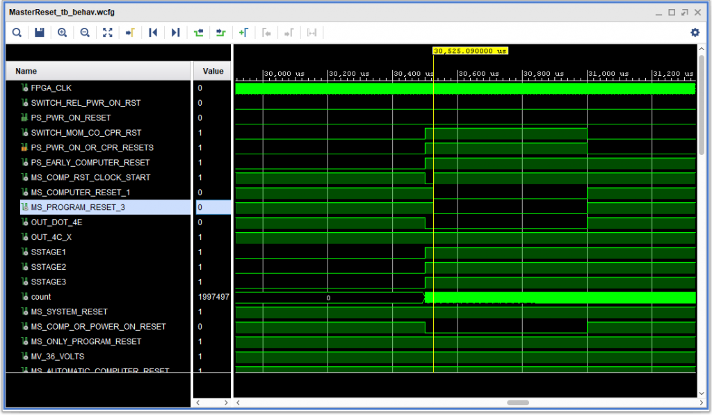
While working on ALD page 12.65.01.1, which generates power on and computer reset signals, I noticed something that didn’t look quite right. The computer reset signal (active negative) when negative when the button push was simulated, then went back inactive, then went active again 25 microseconds later – when it was actually supposed to go active (the result of the timeout of a 25 microsecond single shot gate).
Puzzling – the logic all looked fine. What was going on? At first I thought, “so what – it is going to reset anyway — so no big deal”. But then I looked at the IBM 1410 system fundamentals document, S223-2648, page 26, which makes it pretty clear that the computer reset signal should only be active after the computer reset clock start single shot times out, indicating that the logic gate should stop at either state A or state R. But why?
Then it hit me: CORE STORAGE. If one resets the machine at the wrong time – say, in between reading a character from core (which is a destructive operation) and writing it back, bad things would happen. — the character would be erased. But, how did the actual machine avoid this problem? Sure, I have a relatively long (90 ns, with a 100MHz FPGA clock) single shot setup time to detect the rising edge of an asynchronous trigger on the single shot, but regardless, that setup time would not be 0.
Then I saw it: A 0.047 microfarad capacitor in the ALD page 12.65.0.1 between that computer reset signal and logic ground. Ah HA! A delay!
Fortunately, I had already learned how to implement a delay on an FPGA: with a “bucket brigade” delay line – whose length determines the delay. Sticking a 4 cell (120 ns) delay at that point in the circuit fixed things up just fine.
The results are shown in the simulated ‘scope trace, below. (The count signal and SSTAGE# signals below are for a different 20 millisecond single shot.)
A couple of errors in the IBM 1410 System Fundamentals manual
For starters, I should say that the IBM Field Engineering Instructional materials, which I relied on heavily when creating my IBM 1410 Simulator software are excellent, especially considering these documents were typeset in more than a decade before anyone had heard of a word processor.
Nonetheless, I stumbled into two errors in the IBM 1410 System Fundamentals manual, S23-2589, this week. Both are instances where the output signals from gates are different from what is shown in the document.
The first one I ran into was the first Single Shot that I came across in the diagrams, SMS card type DHE, part number 370262. The timing diagram shown in figure 110, page 93 of the manual shows a negative going input pulse triggering a positive going output pulse. An analysis of the electronics in the first of two SMS card manuals (which have no number) and the use of this card in an ALD, 12.60.20.1, makes it apparent that a negative going incoming pulse creates a negative going output pulse. (This was implemented in my FPGA VHDL generation by triggering a counter on the leading negative going input pulse, which then counts down to 0.)
The other error applies to card type DFZ (and its companion, DGA), which I ran into on ALD page 12.61.13.1. The timing diagram in figure 107 on page 92 of the System Fundamentals manual shows NAND logic: If both inputs are high, the output goes negative. However, analysis of the circuit for DFZ, part number 370241 makes it apparent that it is actually NOR positive logic: If either input is high (approximately 0v), then the output is low. Only if both inputs are low (negative voltage) is the output voltage high. This was “sussed out” by looking at the intended logic on the ILD.
The first missing IBM 1410 ALD Sheet
Ran into the first case of needing to reconstruct an Automated Logic Diagram (ALD) page, as part of my ongoion IBM 1410 FPGA implementation project.
The page for the 2nd and 3rd Scan Controls, 12.30.04.1, was missing from my diagram set. I did have information about how many gates from which cards were present on the diagram, gleaned from the card location charts. Fortunately, the Instructional Logic Diagrams (ILD) covered the missing page. Between the two I was able to construct the page, using the original gates, and other than logic block placement on the printed sheet, I expect it is pretty accurate.
I only hope all of the missing pages are so “easy”. Easy is in quotes because on the 3rd Scan Control latch, there is a collector pullover to logic 1 to reset the latch that is not common. That same situation exists with the same card type (DFA), so I was able to verify the gate utilitzatin.
IBM 1410 ALD Volume II Completed
I have reached a sort of milestone in my efforts to replicate the IBM 1410 Data Processing System in an FPGA. The Automated Logic Diagrams (ALDs) comprise 11 volumes – I through XI. Volume I is power supply and general items, and so does not play into the process very much.
The milestone is that I have completed generating and running HDL test benches on all of the pages in Volume II (except for one, having to do with a clock, which is not critical, and may or may not be addressed later.)
I really am surprised about a couple of things. First, while I have fixed a smallish handful of bugs in the data gathering / HDL generation application, there really have not been very many problems in that area. The second is that, aided with the information in the Instruction Logic Diagrams (ILDs) in my testing, I have found very very few issues with the data that was actually captured – relatively few “clerical errors” – few enough that I am pretty surprised.
On to Volume III!

