Once the 1415 console emulation was up and running, I was able to run diagnostics. The first set of diagnostic failures arose in the Assembly Channel because the Automated Logic Diagrams I had for parts of the Assembly Channel were not for the 1410 Accelerator feature, unlike the vast majority of ALD pages I had.
Once I fixed that, diagnostic CU01 ran OK in non-overlapped non-priority (interrupt) mode. However, once I enabled overlapped I/O with the priority feature in the diagnostic settings, the diagnostic errored out with an Instruction Check. The overlapped I/O is that of the 1415 console. The diagnostic then monitors that (along with a priority interrupt) to make sure that the channel status information and the interrupt operate as expected.
The Assembly Channel issue had been reproducible using a single instruction, and I could set that instruction in the initialization of the first 10K memory module, so I was able to troubleshoot it using simulation. But not this one – it happens after 10s of thousands of instructions. I had been less than confident about using the built-in logic analyzer capability that Vivado affords for Xilinx chips, but this problem left me no choice. Fortunately, after just one false start, I was able to figure out how to make a change in the signals the logic analyzer had available, set triggers, and so on – so, not so bad.
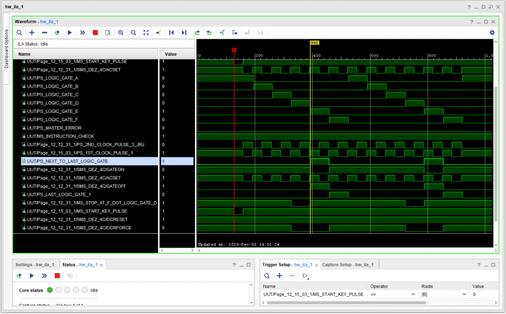
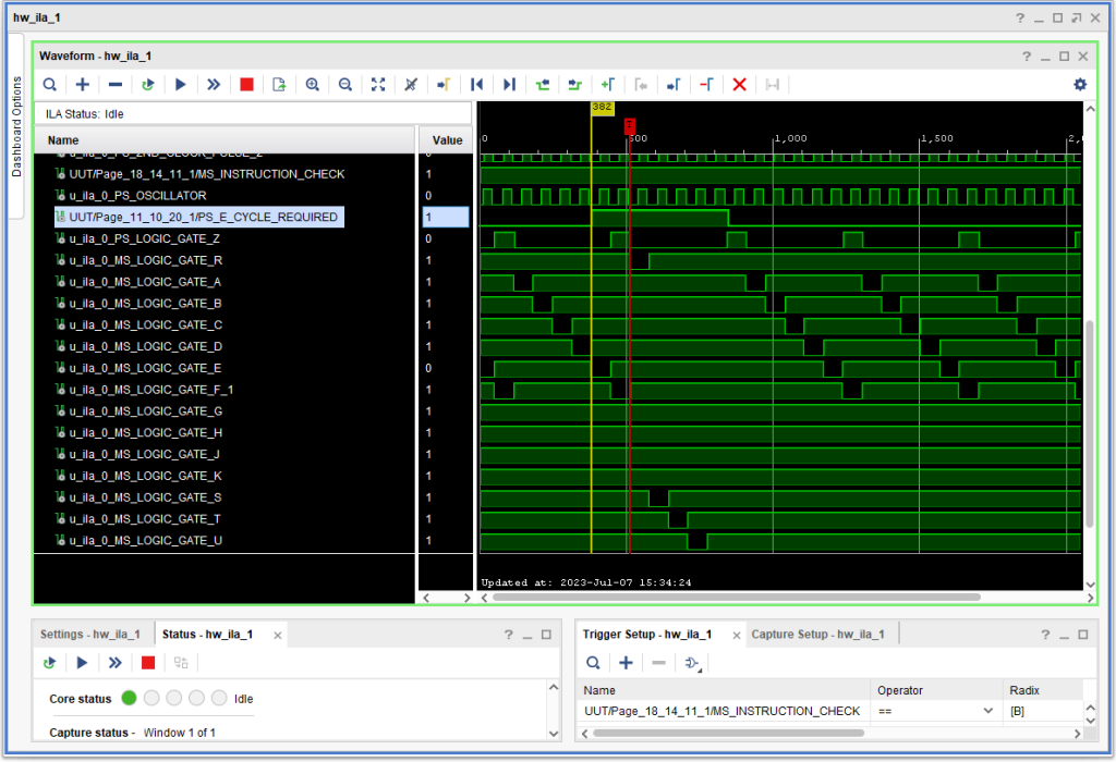
Here is what the problem looked like that caused the Instruction Check. Note that the signal +S E CYCLE REQUIRED is going active (high) just after signal -S LOGIC GATE A. Now, that should not be a problem, except that +S ERROR SAMPLE is also high at this point, and since Logic Gate A is active, as well as E Cycle Required, the logic in the CPU sees that as a possible problem – knowing that if E Cycle Required is active, it ought to be activating Logic Gate R rather than Logic Gate A. (Note: At this point I had not included +S E CYCLE REQUIRED A (one of four different ways that +S E CYCLE REQUIRED can be asserted – and which turned out to be the “villan” in this case. Anyway, here is what the output of the logic analyzer looked like:
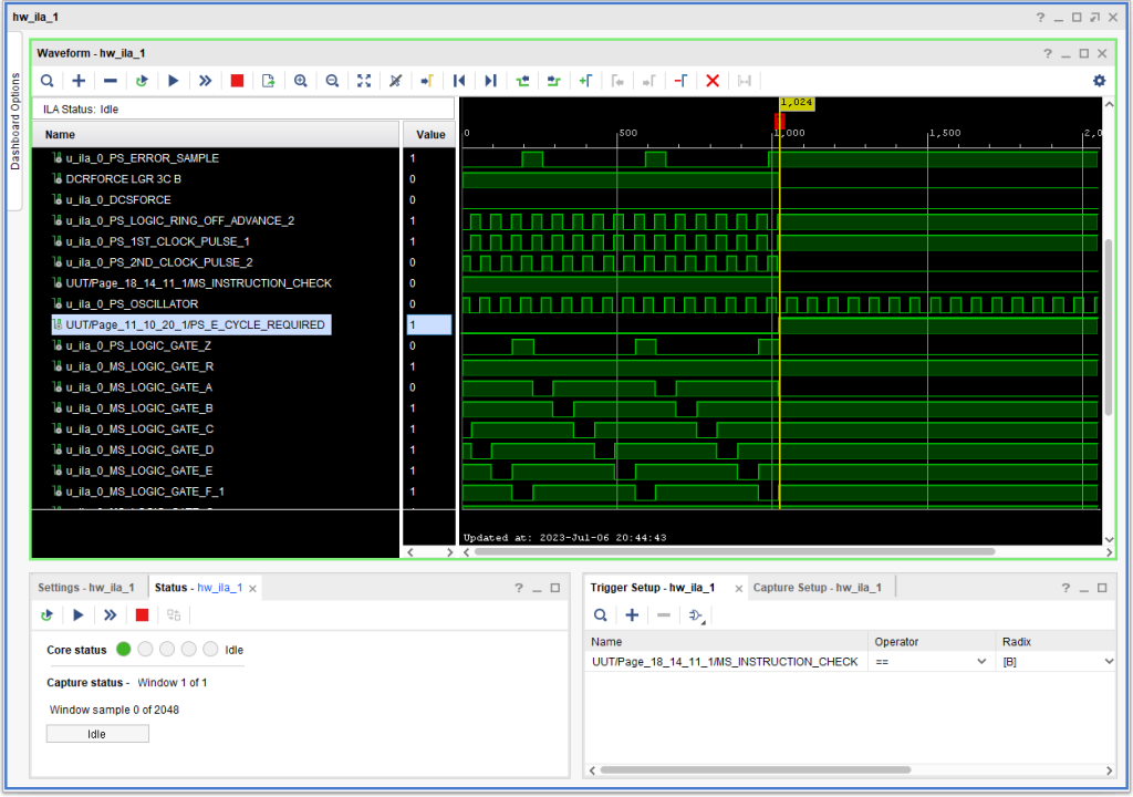
Now, this was not occurring on all or even anywhere near a majority of overlapped I/O operations. Below is an example (using the very same FPGA configuration) of a successful overlap. Note that in this example, +S E CYCLE REQUIRED is asserted much earlier – along with -S LOGIC GATE E so there is no race – E Cycle Required is ready and present long before the time of+S LOGIC GATE Z when the CPU makes the decision between Logic Gate A and Logic Gate R is made.
So, I went looking for possibilities:
- Had I made a mistake when I entered the data for the associated ALDs?
- Was this a race condition caused by the fact that I insert “D” flip flops to disconnect any timing loop identified by my generation code (within a single ALD) or by Vivado during synthesis (involving multiple ALDs)?
- Was this a race condition caused because the FPGA gates are much faster than the original RTL logic SMS cards, and/or the fact that LUTs are used to collapse combinatorial logic into a decision table that may eliminate multiple levels of original gates?
- Was this a very tight timing window in the original CPU?
During my investigation I came upon this tidbit in manual 226-2692, IBM Customer Engineering Instruction-Reference 1411 Input-Output Operations on page 46:
Service Note
Because close timing conditions occur in the areas listed below, excessive delay, or accumulated delays in the logic circuits may cause machine failures:
CHANNEL REGISTERS AND CONTROLS
E-cycle required
F-cycle required
E-cycle control
F-cycle control
Address channel
Well, do any of those look familiar? Like maybe the italicized one? While I have resolved the issue, I do not know, for sure, the exact nature of why I ran into it. The original CPU had the +S E CYCLE REQUIRED signal originating in (physical) Frame “D”, whereas the logic gate signals are created in Frame “C”, a couple of feet apart. As a guess I think it is most likely the the FPGA logic is faster than the original hardware in this area, such that +S E CYCLE REQUIRED could be being asserted earlier than the original engineers thought probable.
Regardless, I faced the issue of what to do about it. I had several choices:
- I could try and tweak my generated logic in terms of speed, by adding delays, to see if I could resolve it that way.
- I could inhibit +S E CYCLE REQUIRED A (the one that seemed problematic) in the presence of -S LOGIC GATE A so that in such a case, the E Cycle Required signal would not be asserted until near the end of the memory cycle of this enar miss.
- I could inhibit +S E CYCLE REQUIRED (so, all four possibilities) in the presence of -S LOGIC GATE A
The first two choices might work, but would leave me in a situation where this problem could recur later on, in some other setting, whereas the third option would prevent it from happening a priori. The only downside that I could see would be that it might prevent a device from transferring data to memory quite as fast as the original.
So I investigated transfer speeds of various devices to see what they might be like:
- Unit record devices have a core buffer in the IBM 1414 I/O Synchronizer, and are slow enough anyway, that it would not likely make any observable difference.
- IBM 729 tape drives. The 729 IV transfers at 112.5 IPS at 556 CPI, the 729 VI at 112.6 IPS at 800 CPI. So, roughly, 112.6*800 = 90,080 cps, or a bit over 11 micro-seconds per character. So, every other cycle would be fine on a an 1410 with the Accelerator feature with 4.0 microsecond cycles – allowing it to “steal” every other core cycle.
- IBM 7340 Hypertape Drives. Some models are 112.5 IPS / 170,000 cps tape drives (so, roughly 1500 CPI), or 5.9 microseconds/character. That would require making transfers in non-overlapped mode (see the 1302 disk drive, below). However, ones attached to a 1410 more likely operated at 34,000 cps – plenty slow enough.
- A 1405 Disk Drive spins at 1200 RPM (so only 20 rps) and has a 1000 character track size (so, say 1200 to be conservative). That gives us about (1/20)/1200, or 50ms/1200, or 41 microseconds per character – lots of time.
- A 1301 transfers characters at 90,100 cps, or 11 microseconds per character – so plenty of time using every other core storage cycle.
- A 1302 transfers characters at 184,000 cps, or 5.4 microseconds per character. But on a 1410, these devices transfer data only in non-overlapped mode (even if the I/O instruction specifies overlapped mode) – because they must use consecutive storage cycles for their data.
- A 1311 (the 2311 is not supported) has 2980 characters/track, and rotates at 40ms/revolution. this gives us roughly 13 microseconds per character.
These point to things being OK so long as the peripheral can “steal” every other core cycle. On top of that, the 1410 Channels are double buffered, so even if sometimes it takes 5 cycles to get two characters in or out, operation should not be affected. It would not seem the peripheral speed would prevent using the last option listed.
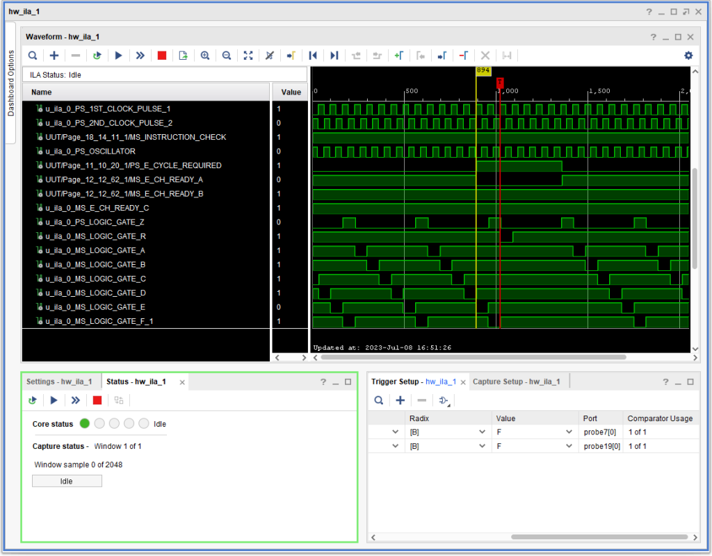
So, I made the changes, labeling them with a fictitious ECO “JRJ001” in the database and tested – diagnostic CU01 now passes without problems. Below is what the signals look like, timing wise. I believe (but cannot prove) that what happened is that +S E CYCLE REQUIRED ended up delaying until the next possible “last logic gate” (in a given memory cycle), which is typically logic gate E, as is the case in this capture.
So, what is next on the block?
- Several enhancements to the console program, including merging what is now the main root window with the 1415 console form – no need to have them separate.
- Run more diagnostics, by saving core images under my software simulator and transferring them to the FPGA memory to read them, as I did with CU01.
- Experiments with speeds: how fast can I run the 1411 CPU before it fails its diagnostics?
- Research into channel signals. I don’t have ALDs for the relevant IBM 1414 I/O Synchronizers, though I do have ILDs, which pretty well define the logic. But rather than parroting exactly what the 1414s would have done, I will likely just use VHDL using some of that ILD logic as a wrapper around communication to and from the PC support program, at least at first.