Tomlov DM-201 Digital Microscrope Review

I purchased this microscope with two applications in mind. First, primarily, to use when soldering SMT devices onto circuit boards. Secondarily, I wanted to see if I could read and capture images of 1960’s era manuals that are on microfiche.

Overview

Firstly, I want to mention that the level of support I received from the email address provided with the unit exceeded my expectations.

Questions on the Amazon listing were answered within 24 hours, as were email questions after I purchased the unit. Most of them related to the limitations on still frame capture I discuss, below.

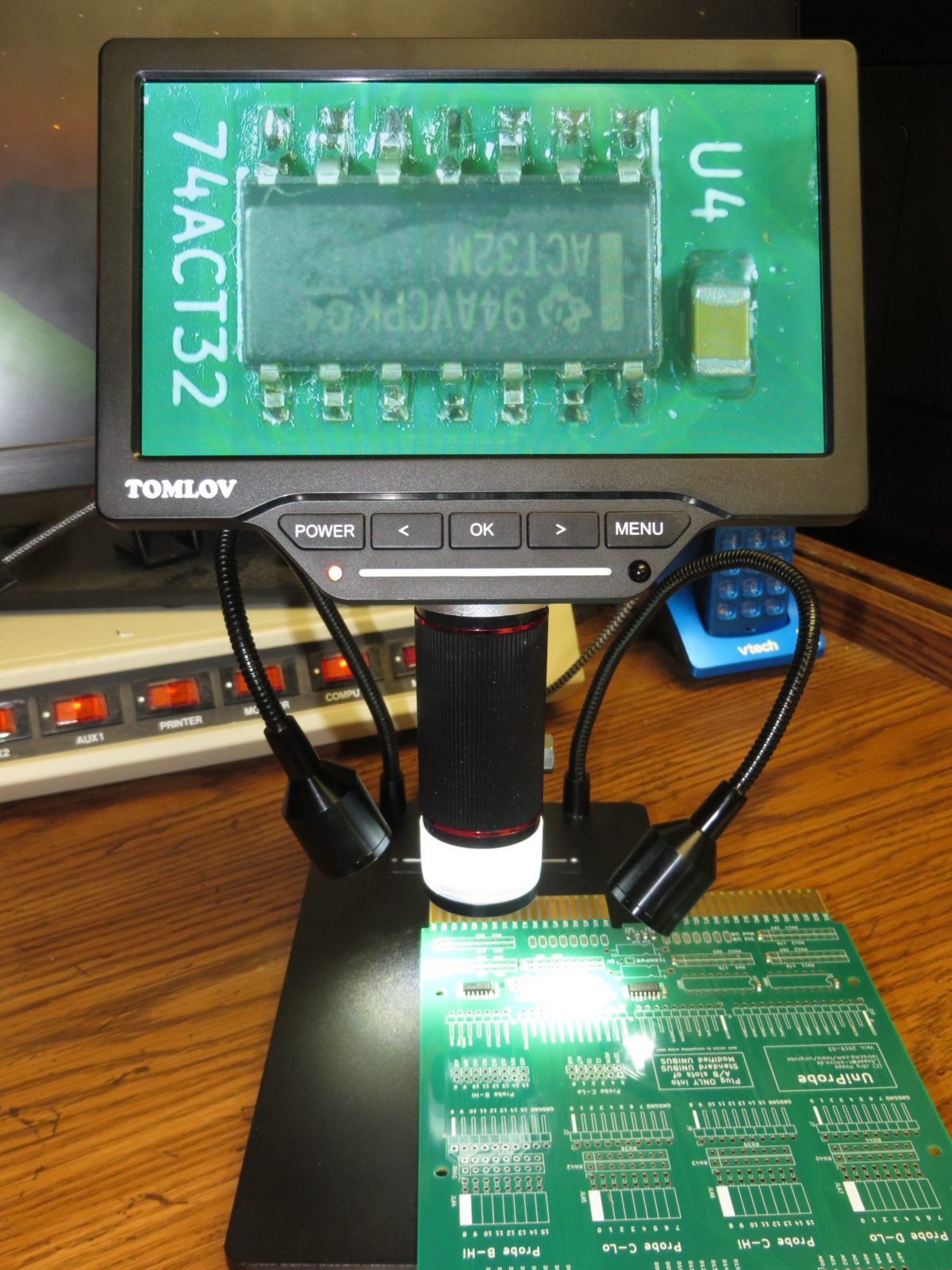
The 7 inch (diagonal) screen is nice, and the post arrangement allows a wide range of zoom factors for soldering, down to individual pins. The camera is easy to use, and can stream video directly to an HDMI monitor via its “mini” HDMI connector, and can be connected to a PC as well. Images were clear and sharp on the monitor and in saved images of circuit boards.

Battery life seems pretty good – more than a couple of hours. I did not quantitatively measure it.

Overall, the device serves the primary purpose quite well.

Note that this unit was purchased by me: it was not supplied by the vendor for review.

Camera Lens and Sensor

This device features a VMS700 camera, with a 4 mega pixel (MP) native resolution, which the firmware can extend to 16 MP using interpolation, which does help clarify the images a little bit. According to the web page for the product, the post on the stand can be tilted from upright to an angle, though I have not actually tried that. Color depth is 24 bits per pixel.

The lens provides a wide range of zoom capabilities. Using the shorter post on my unit, without the included extender, the zoom is probably something like 1X – 300X; using the new taller post the Tomlov web site indicates it has a zoom range from 1X to 1200X. The middle of the lens is a fairly large focus ring – more than an inch – making it very easy to use. A glass filter – probably a UV filter – is also included with the setup.

Base and Lighting

My unit came with a screw on extender for the post to raise the camera higher from the base (not shown in my photo), which is a little inconvenient to use, but recently the DM201 was updated with a taller post that does not require unscrewing and reattaching the mount to add the extender – a nice improvement. Tomlov offered to send me this updated post, but I declined as I did not need it for my purposes.

There are three different light sources on the unit. The first is a ring light built into the camera lens assembly. The brightness is adjustable from fully off to fully on in steps using a little (lighted) bar just below the buttons on the LCD screen. It can be adjusted either by sliding your finger on the bar below the screen, or tap the bar on the left or right side – the latter worked better for me. There are also two lights built into the base, and a similar control for them near the back of the base. The base gets its power for these lights via a provided USB micro cord that runs from the USB “A” type connector on the back of the screen assembly down to the USB “C” connector on the base.

IMPORTANT TIP: If you want to take an image of a transparency (say, a slide or microfiche) then you have to position a light source underneath the transparency. I purchased an inexpensive ($15-$20 US) thin LED light table / tracing table for that purpose, leaving the microscope’s own light sources turned off.

Connections and Remote

Besides the USB “A” connector, the back of the screen assembly has a “mini” HDMI connector, a micro SD card slot – the SD card was included and already in place in the unit I purchased via Amazon, and a USB “C” connector for charging the screen unit and attaching to a PC.

Besides the LED slide control on the front, the front of the screen assembly also has a power button, four menu control buttons, an LED to indicate power / charging status, and a sensor for controlling the unit via an infrared remote, which I did not test out. But the remote would be important for capturing high quality still images to the SD card so that the lens does not move as when pressing the “OK” button, which is the other way to initiate a still image capture.

Connection to a PC allows access to the camera via the UVC (USB Video Class) interface on Windows. By pressing the OK button, one can switch from UVC to MSDC mode, which supports access to the CF card on the device as a Windows “disk”.

Settings

The menu supports a number of settings, including:

  • Playback of existing captured still images or videos (I did not test the latter)
  • Management of existing capture files (this can also be done from the PC over MSDC)
  • Control of exposure (automatic or manual/lock),
  • White balance (automatic, manual or to calibrate), or set specific R/B/G values
  • Image type: Color “B/W” (which is really greyscale) and Color Negative
  • A Wide Dynamic Range setting, which the manual says works better if you have light and dark areas together
  • Contrast (only if Wide Dynamic Range is turned OFF)
  • Saturation and Sharpness
  • Flipping the image horizontally or vertically (I wish they had 90 degree rotate as well)
  • Frequency of 60Hz of 50Hz (presumably the vertical refresh frequency for the HDMI and USB video outputs?)
  • Setting the mode, Photo, Video, or “Freeze” which lets you capture images and displaying them next to each other
  • Video output, for 1080P30 or 720P60
  • For freeze, whether you want to save one, 1/2 or 1/4 of each image you take
  • LCD brightness
  • Auto off: none, 1M, 3M or 5M
  • Language: Choose from English, Chinese, Japanese, Russion, German, French, Spanish or Portugese
  • Reset to default settings
  • Format an SD Card
  • Current version (mine was version 1.2.19)
  • There are also a set of controls for controlling reference lines, which I did not try out

Limitations

While using this device to do some SMT soldering and capturing of images off Microfiche, I did find some limitations:

The still frame camera images at native 4MP or interpolated 16MP resolution are only accessible via the SD Card or MSDC. You can capture still images using the Windows built-in Microsoft Camera app, but those seem to actually be single frame captures at HD resolution (1920 x 1080) off of the video stream. I found I could not successfully capture still images using a demo of the commercial AMCap application — I got a black image with the expected watermark. Fortunately, access via MSDC works well, and you can even delete images or videos on the SD card from the PC that way.

You cannot access the menu to changes settings while connected to a PC in either UVC or MSDC mode.

The screw down retaining ring that holds the post to the base doesn’t work as easily as one might wish – you have to work a little to turn it down so that the post is firmly mounted.

Unfortunately, there is no way to disable the JPEG compression when saving still images to the SD card, which might be useful for post-processing those images.

When I set the zoom to capture an entire 8.5″ x 11″ “page” from the microfiche I had, rotated on its side for the best fit, it comes out at an effective pixel density of about 178 dots per inch at the 4MP 2688×1512 native resolution (1512 / 8.5″). Unfortunately, this provided a bit insufficient for my needs. I would need at least 8MP native resolution to get to the requisite 300 dots per inch.

The base lights can be a bit tricky to get pointed exactly where you want them. Sometimes one has to pinch them quite a bit to get them to stay where you want.

Sample Images

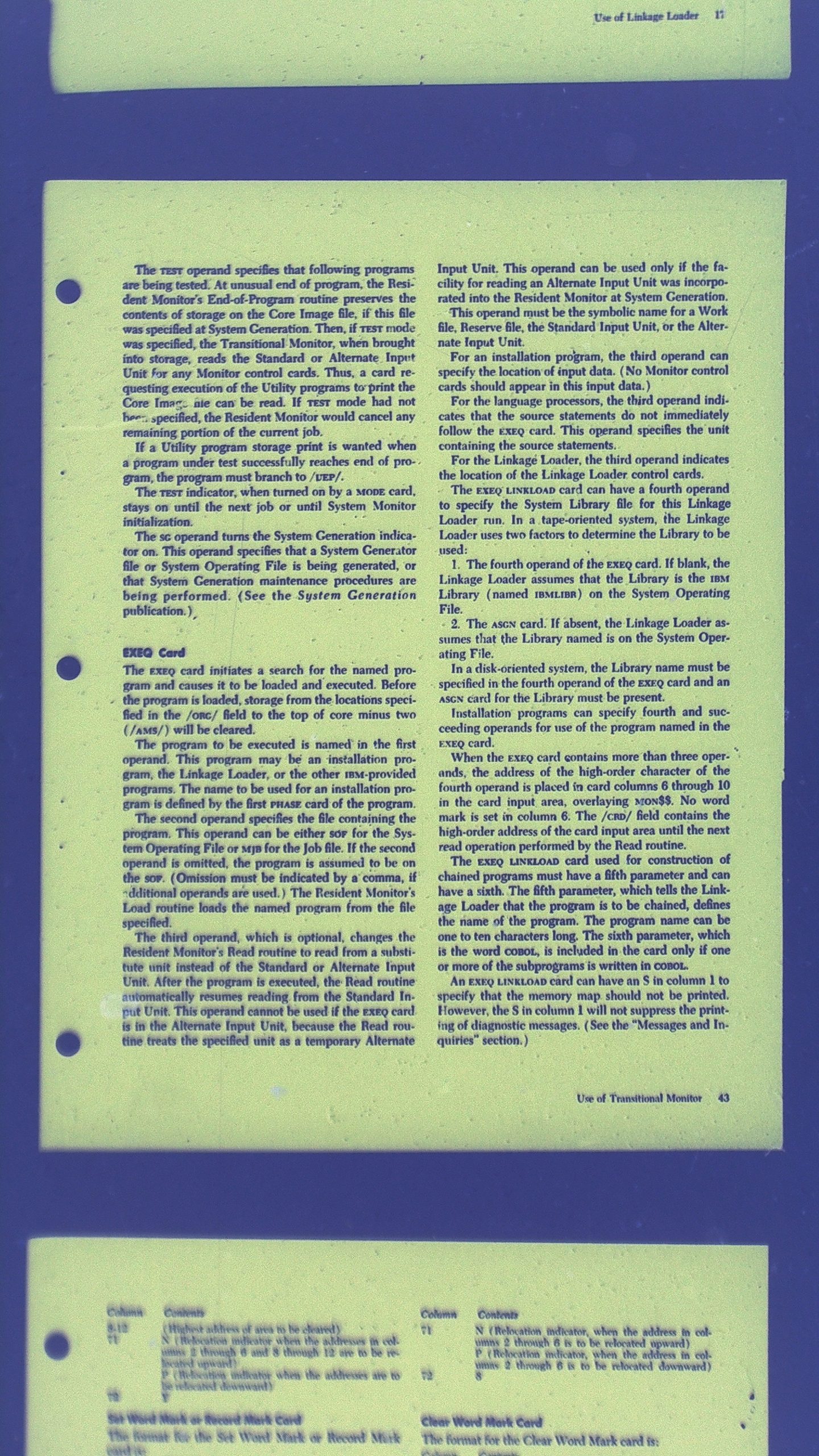
The first image is a 4 mega pixel native sensor resolution image captured and transferred from the microscope’s SD card. The second is a 16 mega pixel image with interpolation by the camera’s firmware. All but the last set are effectively what what might see from a 175 dpi scan of the original document.

Note that I didn’t have any glass on top of the microfiche while I made these, so the areas at the top and bottom edges of the page scanned, and beyond, particularly, are somewhat out of focus.
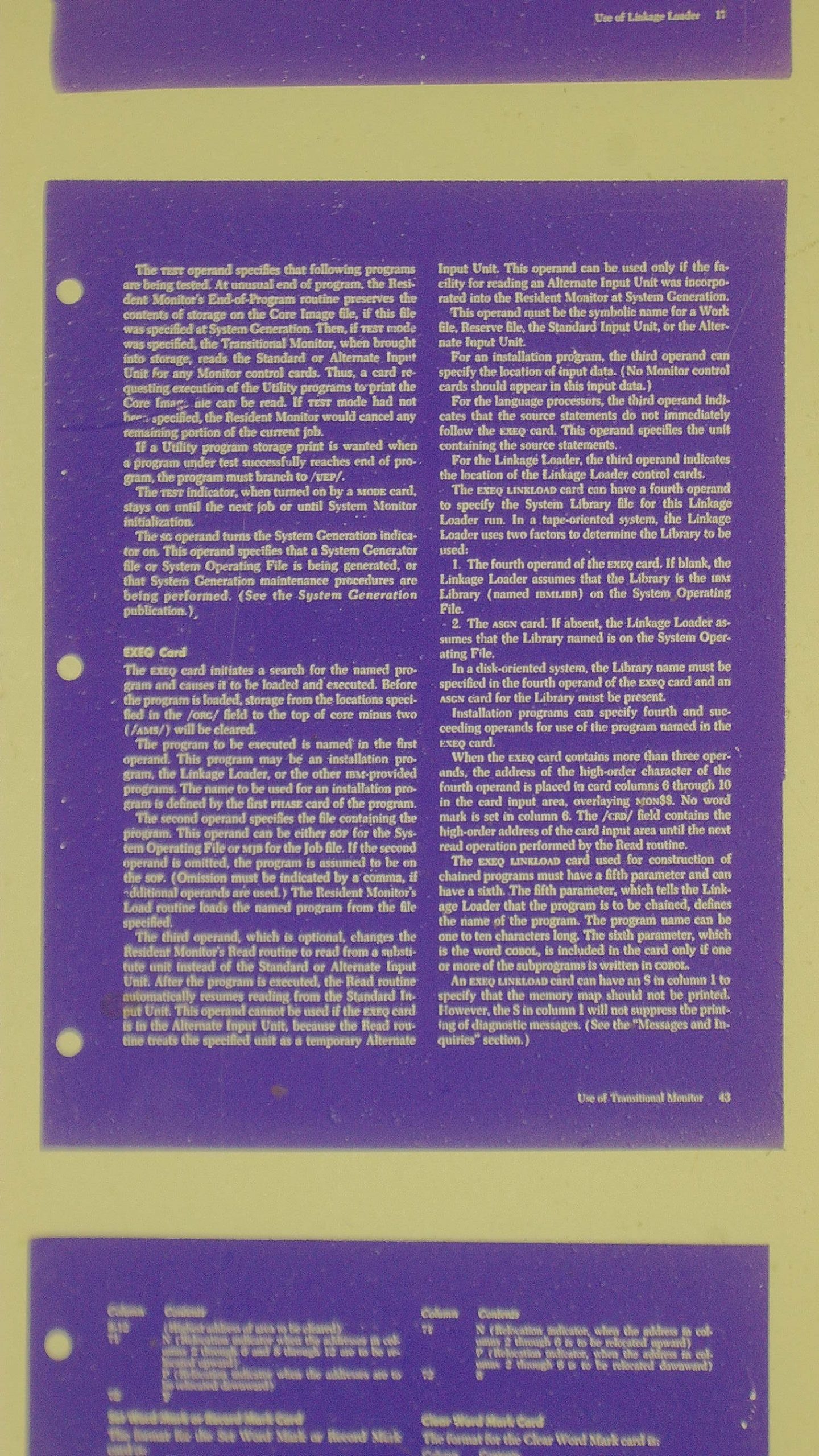
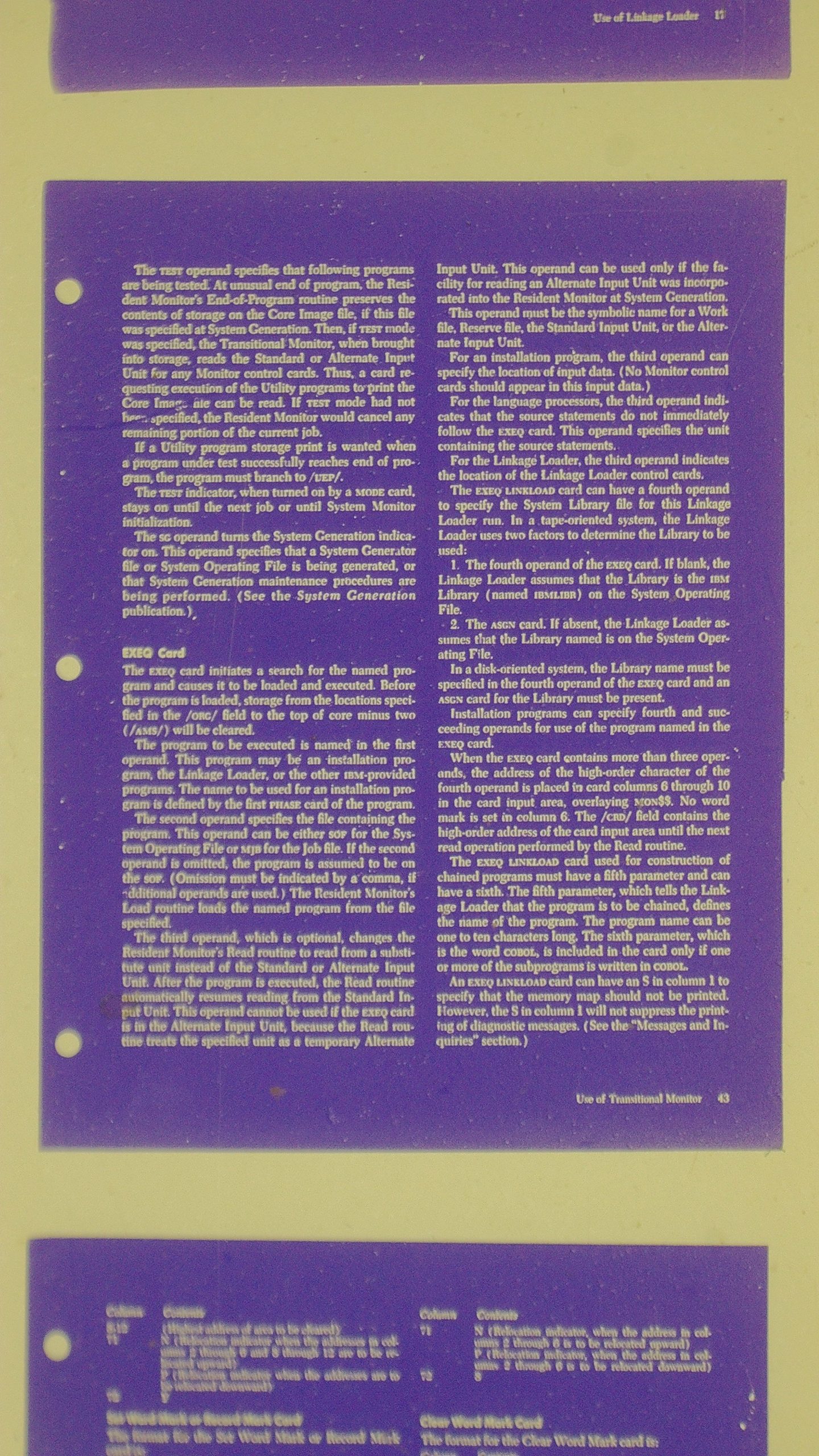
Above, a 4 Megapixel Color captured image, uncropped.
Above, a 4 megapixel color captured image, uncropped.
16 Megapixel Color captured image (interpolated), uncropped
16 megapixel color captured image (interpolated), uncropped

Next come the 4 and 16 mega pixel images, as color negatives.
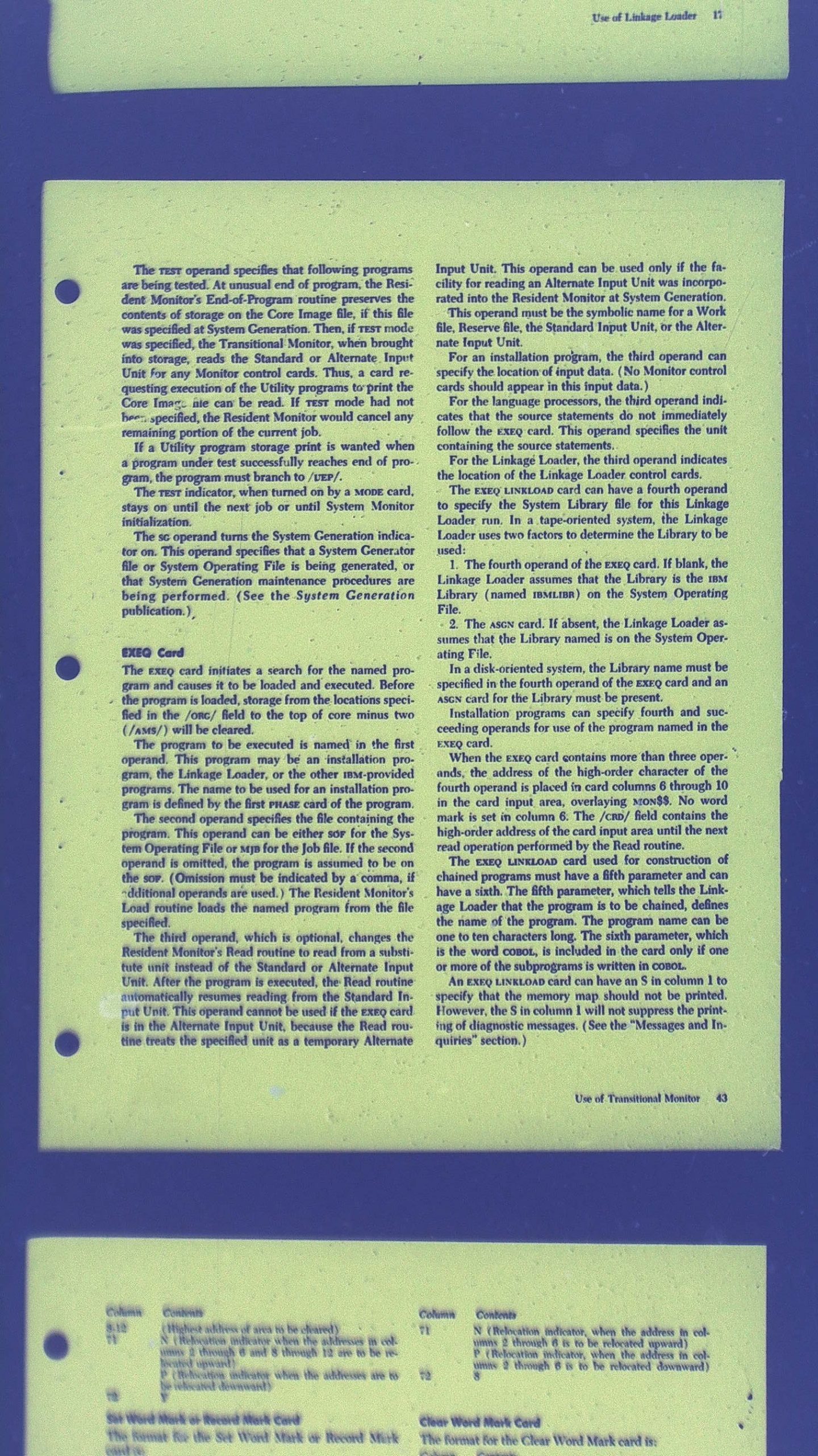
4 Megapixel image, color negative, uncropped
Above a 4 Megapixel captured image, color negative, uncropped
16 megapixel color negative captured image (interpolated), uncropped

Finally, some “Black and White” (24 bit gray scale) images.
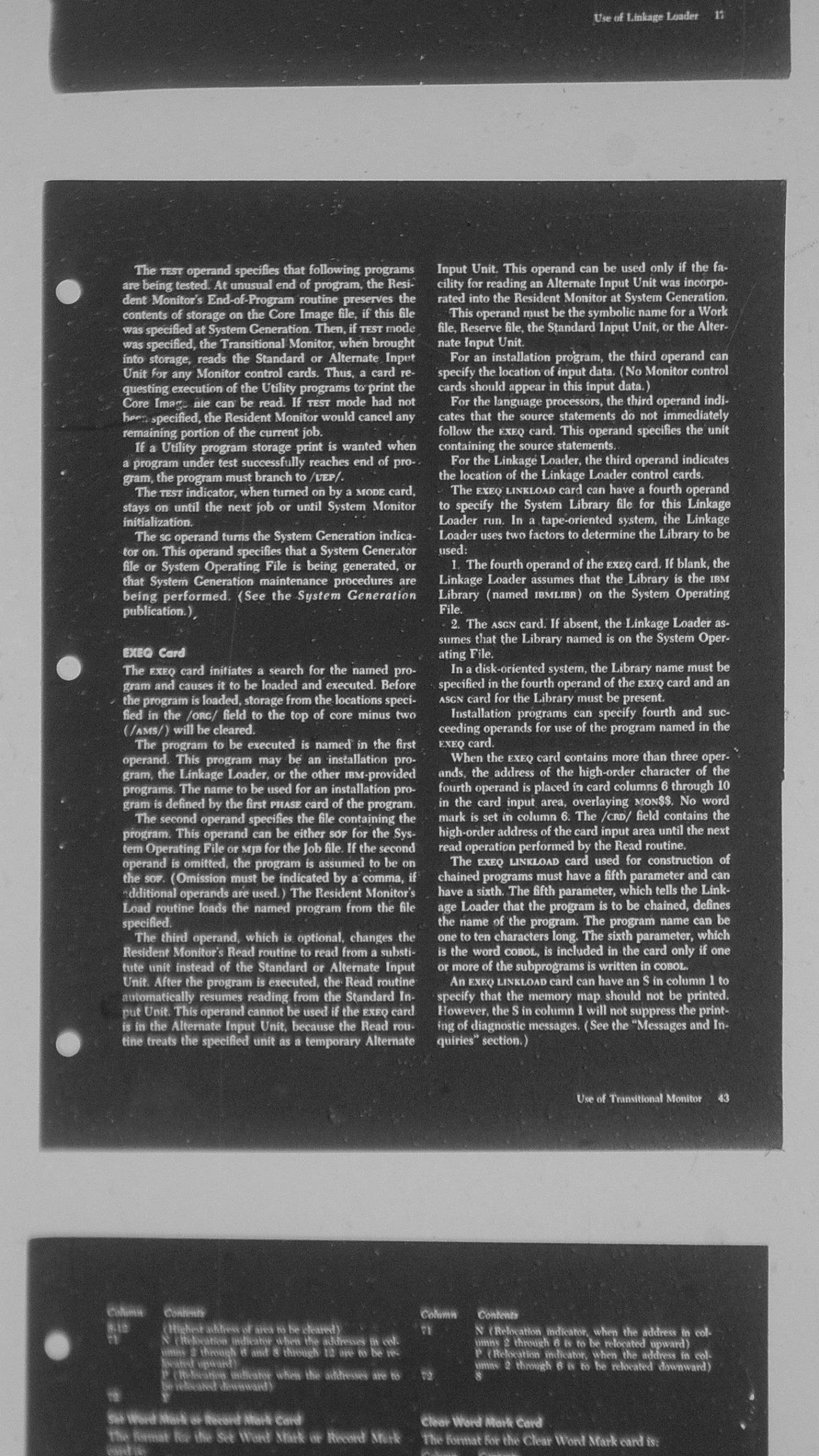
4 megapixel image, gray scale, uncropped
4 megapixel captured image, gray scale, uncropped
16 megapixel captured image (interpolated), gray scale, uncropped

Finally, the following images are with the lens fully zoomed in (moved on the post down right next to the microfiche. These would effectively be something around 400 dpi with respect to the original sized document – but only a partial document is in the field of view.
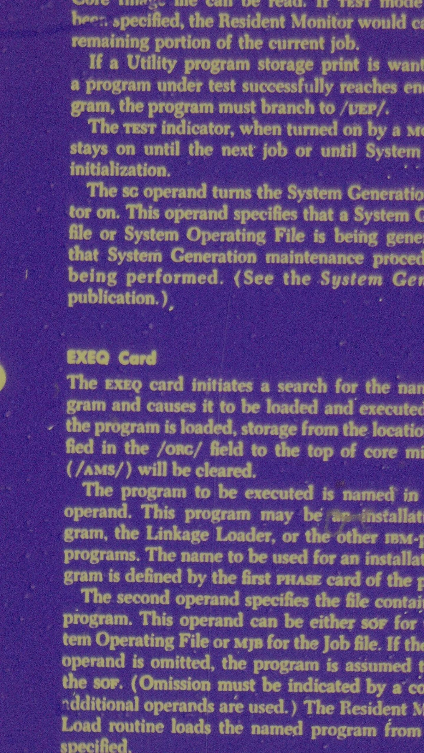
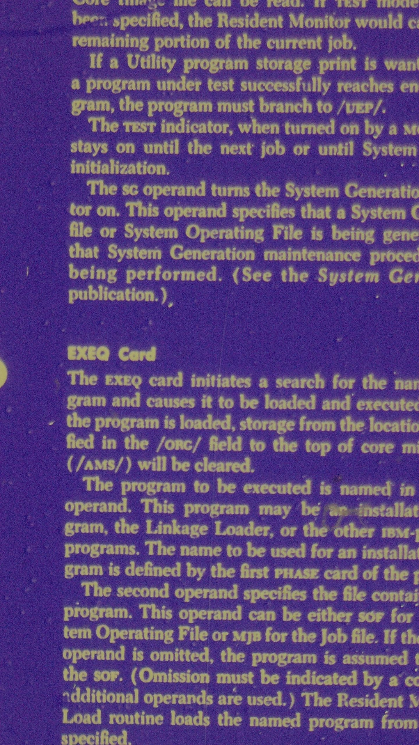
4 megapixel color capture fully zoomed in
16 megapixel (interpolated) color capture fully zoomed in
16 megapixel color capture fully zoomed in

IBM 1410 FPGA: Posted to Github

The last 12 months I have been pretty busy working on my 1410 in FPGA project, and there is now more to share, though I have not done much actual work since February – been too busy playing with other “toys”.  8D

First, I finished working through all of the IBM 1410 and IBM 1415 Automated Logic Diagrams – generating VHDL and testing the results with test benches.  [Note that this includes the built-in 1401 compatibility mode, activated at the flip of a switch.] That took most of 2020.

So, the CPU generation in VHDL is now more or less complete, and I added a hand coded memory module for memory, as core is kind of hard to find on an FPGA development board.  😉  I am currently using a Digilent Nexys 4, but I think it might have even fit on a Nexys 2 – there is plenty of room to spare, and there isn’t anything in the VHDL aside from, maybe, the memory implementation (though even that is pretty generic VHDL).

With this the CPU runs, at the very least, Unconditional branch (Jump), Halt, NOP and Set Word Mark instructions seemingly correctly – I haven’t tried any others.  Somewhat surprisingly, aside from issues with the hand coded VHDL in triggers and the need to communicate pins tied to logic one or zero, the auto-generated VHDL works untouched.

I have updated the github repository for the C# database application that generates the VHDL from time to time (and which includes the complete database) at http://github.com/cube1us/IBM1410SMS

There is now a *new* repository, http://github.com/cube1us/IBM1410FPGA which holds the generated VHDL, some hand coded VHDL modules for certain SMS cards (typically for triggers, for example), the console and test benches I used along the way, and VHDL “Integration Tests” which are designed to be loaded onto the board – the current one being IntegrationTest3.

There will be, eventually, a third repository which will contain the C# code that “hosts” the IBM 1410 console and peripherals, communicating with the FPGA over a high speed serial over USB connection.  I figured out that this should allow me to emulate peripherals without having to resort to sending data over Ethernet, SPI, I2C or the like.  I have just started that, so it really isn’t at a point that there is much to share.

Once I have a console working (which will require a re-do of the console VHDL implementation, which right now communicates in ASCII, but should probably be using BCD), I should be able to pre-load into memory some of the CPU diagnostics, by loading a diagnostic routine into either my 1410 simulator (http://github.com/cube1us/1410), or Richard Cornwell’s emulator in SimH and then taking a snapshot of “core” to pre-load into the FPGA.  At that point I expect I will be able to test the CPU pretty thoroughly.  I hope and expect that will happen this year sometime.

Unfortunately, I do not have the ALDs (Automated Logic Diagrams) for the IBM 1414 I/O Synchronizers, but I do have the Instruction Logic Diagrams which should allow me to code VHDL to emulate card, tape and maybe eventually even disk functions, so those might take a while.

Finally, a Radio Antenna

Over the past couple of months I have been working planning, and now, this last week, installing a radio antenna suitable for Ham frequencies (in particular, 10, 20 and 40 meter wavelengths).

The antenna installation comprises:

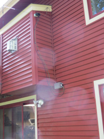
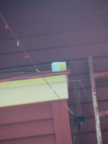
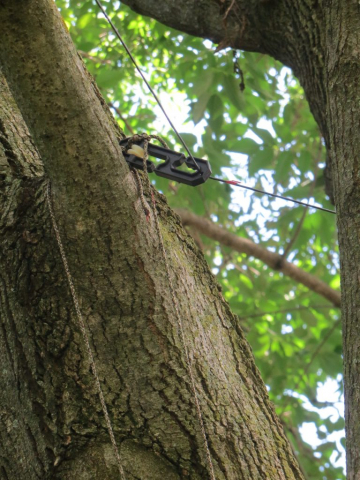
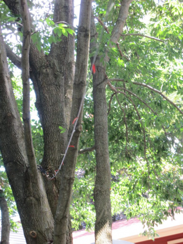
  • A 60′ plus antenna wire, run from our cut-off chimney, then passes though a tree supported from a limb, and then is attached via a rope to a 10 foot high PVC pipe which is sunk into the ground 2 feet, which provides support for the far end (and keeps it well above my head.)
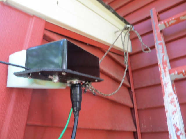
  • An antenna matching transformer that matches the relatively high impedance of this “end fed dipole” antenna to the 50 ohm impedance of the coax feed line attached to it.
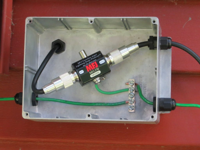
  • A safety ground the leads down from the box containing the antenna matching transformer, to a metal box which connects this to the lighting arrestor ground and a ground that runs off to the inter-system ground (see below.)
  • A lightning arrestor which is installed into the feed line, and which connects to the feed line into the house.

A big difficulty with my antenna installation was grounding. An antenna must have a ground, both to “work”, but also to provide static discharge to discourage lightning strikes.

If lighting strikes a typical antenna, it will vaporize and likely damage any equipment attached to it – that is not what the safety ground is designed to prevent. Rather, it attempts to discharge pre-lightning voltage build-ups.

An ideal ground is directly below the antenna, with a 6 foot or so rod driven into the soil. However, if that is done, it is also crucially important to “bond” that ground rod with any others on the property (such as one installed by the electric company.) The reason this is so important is that if lighting strikes the utility lines, it wants to find its way to ground, and will happily do that through your house wiring to find your radio ground, if the two ground rods are not bonded. The reverse is also true if lighting strikes the antenna.

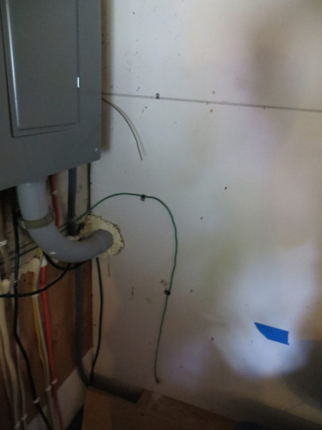
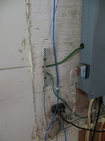
However, in my case that would have meant running the AWG 6 (!!) bonding wire through a rock wall, which was rather impractical. So, instead, I opted to run the safety ground above ground, mounted under the deck, and connect up to the inter-system ground that was installed at my electrical panel in 2017 when that panel was replaced. That connection then connects it to the utility ground rod.

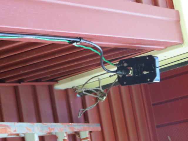
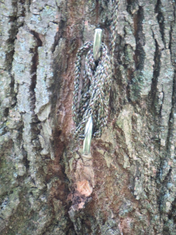
Here are some photos:

Note that the antenna box in the first picture, which contains the matching transformer, attaches to the eye bolt on the chimney with two lines of different lengths. Do you know WHY the lengths are different??? Leave a comment, below.

Q: When is a Capacitor not “just a capacitor”

A: When it is acting as a simple delay line

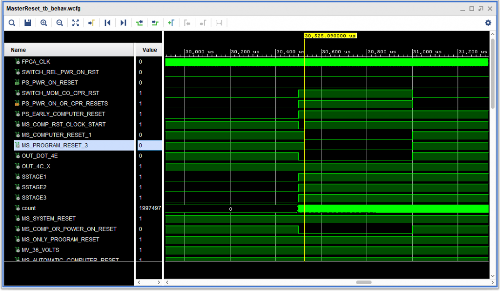
While working on ALD page 12.65.01.1, which generates power on and computer reset signals, I noticed something that didn’t look quite right. The computer reset signal (active negative) when negative when the button push was simulated, then went back inactive, then went active again 25 microseconds later – when it was actually supposed to go active (the result of the timeout of a 25 microsecond single shot gate).

Puzzling – the logic all looked fine. What was going on? At first I thought, “so what – it is going to reset anyway — so no big deal”. But then I looked at the IBM 1410 system fundamentals document, S223-2648, page 26, which makes it pretty clear that the computer reset signal should only be active after the computer reset clock start single shot times out, indicating that the logic gate should stop at either state A or state R. But why?

Then it hit me: CORE STORAGE. If one resets the machine at the wrong time – say, in between reading a character from core (which is a destructive operation) and writing it back, bad things would happen. — the character would be erased. But, how did the actual machine avoid this problem? Sure, I have a relatively long (90 ns, with a 100MHz FPGA clock) single shot setup time to detect the rising edge of an asynchronous trigger on the single shot, but regardless, that setup time would not be 0.

Then I saw it: A 0.047 microfarad capacitor in the ALD page 12.65.0.1 between that computer reset signal and logic ground. Ah HA! A delay!

Fortunately, I had already learned how to implement a delay on an FPGA: with a “bucket brigade” delay line – whose length determines the delay. Sticking a 4 cell (120 ns) delay at that point in the circuit fixed things up just fine.

The results are shown in the simulated ‘scope trace, below. (The count signal and SSTAGE# signals below are for a different 20 millisecond single shot.)

A couple of errors in the IBM 1410 System Fundamentals manual

For starters, I should say that the IBM Field Engineering Instructional materials, which I relied on heavily when creating my IBM 1410 Simulator software are excellent, especially considering these documents were typeset in more than a decade before anyone had heard of a word processor.

Nonetheless, I stumbled into two errors in the IBM 1410 System Fundamentals manual, S23-2589, this week. Both are instances where the output signals from gates are different from what is shown in the document.

The first one I ran into was the first Single Shot that I came across in the diagrams, SMS card type DHE, part number 370262. The timing diagram shown in figure 110, page 93 of the manual shows a negative going input pulse triggering a positive going output pulse. An analysis of the electronics in the first of two SMS card manuals (which have no number) and the use of this card in an ALD, 12.60.20.1, makes it apparent that a negative going incoming pulse creates a negative going output pulse. (This was implemented in my FPGA VHDL generation by triggering a counter on the leading negative going input pulse, which then counts down to 0.)

The other error applies to card type DFZ (and its companion, DGA), which I ran into on ALD page 12.61.13.1. The timing diagram in figure 107 on page 92 of the System Fundamentals manual shows NAND logic: If both inputs are high, the output goes negative. However, analysis of the circuit for DFZ, part number 370241 makes it apparent that it is actually NOR positive logic: If either input is high (approximately 0v), then the output is low. Only if both inputs are low (negative voltage) is the output voltage high. This was “sussed out” by looking at the intended logic on the ILD.

The FPGA Simulated IBM 1410 has a “pulse”

Having spent the past few months cleaning up my IBM 1410 SMS database program, and posting it to github at https://github.com/cube1us/IBM1410SMS , I have spent the past couple of weeks focused on the HDL (currently VHDL) generation, using GHDL and Xilinx’s Vivado toolset, with an eventual destination of my Digilent Nexys4 FPGA (Field Programmable Gate Array) board.

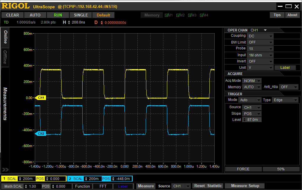
After fixing a few bugs, and implementing the oscillator (by way of a counter/divider from the 100 MHz FPGA clock), I loaded the results into the FPGA, and as show below, my IBM 1410 now has a clock, running at the right frequency for an IBM 1410 with the accerated throughput feature, as shown below:

IBM 1410 FPGA Clock
IBM 1410 FPGA Clock

On the original machine the lower signal, on channel 2 of the oscilloscope, was derived from the first using a delay line – about 330 ns of delay. Kinda hard to do with an FPGA. 😉 So, I implemented delay lines using a series of flip flops clocked by the 100 MHz FPGA clock – so, in this case, there are 33 of them.

This signal is not simulated – it is a real signal that exists in the FPGA.

Change in Amateur Radio Call Sign — W9IYN

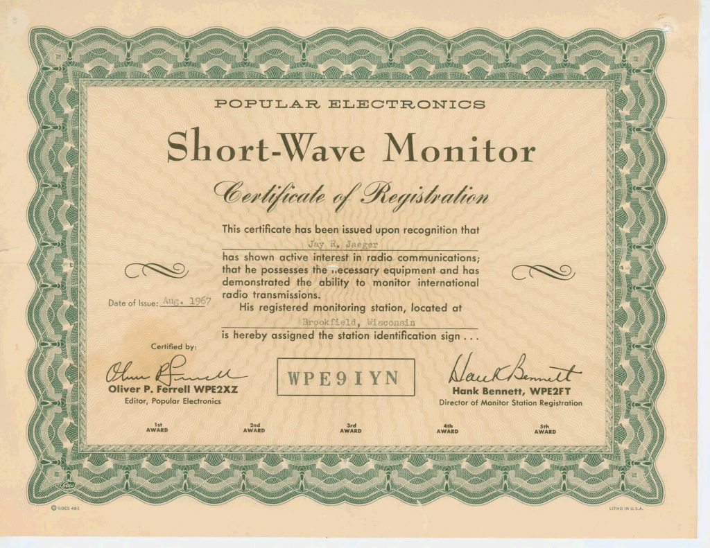
WPE9IYN Shortwave Certificate

Back in “the day” Popular Electronics magazine offered certificates for what it called “Short-Wave Monitor Certificate of Registration”. In the 1960’s I wrote in and obtained such a certificate and was assigned “station identification sign” WPE9IYN.

Part of the “deal” was that Popular Electronics also worked with the FCC to reserve the id (without the “PE” in the middle) so that your assigned station identification sign could also become your amateur radio service call sign.

I had intended to work towards an amateur radio license – my uncle and cousin were Hams. I spent some time learning code, but never actually took the exam.

So, after I obtained my license in February, I checked if W9IYN was available, and sure enough, it was. So, I applied for, and obtained that call sign as a “vanity” call sign. So, my Amateur Radio Service call sign is now W9IYN.

After some 53 years, I am finally a licensed Amateur radio operator (“Ham”)

When I was in middle school, my buddy Ross introduced me to the world of electronics by lending me his Knight Kit “Ocean Hopper” regenerative radio. We also worked together building a flip-flop circuit provided to us by a “traveling roadshow” on computers when we were in 8th grade.

When I was in 9th grade – junior high at the time – I was fortunate to receive the requested Knight Kit “Star Roamer” as a Christmas gift – still have that radio today.

In 1967 I wrote into Popular Electronics magazine, which was offering “call signs” as a “Short-Wave Monitor Certificate of Registration” for non-licensed receive-only hobbyists. At the time, they also coordinated with the FCC to reserve those call signs. I still have my certificate, and will eventually post it on my site.

Fast forward to Feb, 1, 2020, when I took the Technical and General amateur radio exams administered by the Volunteer Examiners from the Four Lakes Amateur Radio Club, and passed both with perfect scores.

My call sign was originally KD9OVL. However, I also applied for an FCC “vanity” call sign – which is the same as the one issued by Popular Electronics in 1967 (without the “PE” portion, after the “W” prefix.). I’ll let you know how that turns out. 😉

UPDATE: As of 3/10/2020, my call sign is now W9IYN.

73 (Amateur Radio lingo for “Best Wishes”)