Additional work has resulted in another step forward in my efforts to reproduce the IBM 1410 (in particular, the IBM 1411 CPU component) in an FPGA.
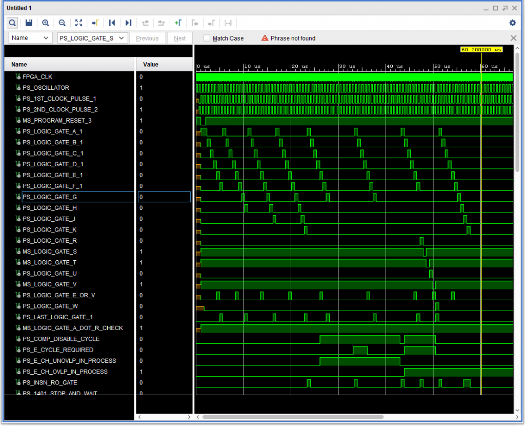
I now have pages 11.10.0*.1, 11.10.10*.1 and 11.10.20*.1 generated and tested (see the image, below).
One very hopeful sign is that easily 90% of the effort in the last couple of days was enhancing the application to preserve a section of VHDL declarations in a test bench, and debugging VHDL test bench code. The generated HDL had performed nearly flawlessly.
In the image below one case see the following (MS… signals are a translation of -S IBM signals – active low. PS are +S – active high.
- The simulated 100 MHz FPGA clock
- The 1.5 MC (MHz for you modern people) system oscillator
- The two phase system clock pulses
- A test bench provided MS_PROGRAM_RESET_3 signal, provided by the test bench.
- The logic ring gates A through K and R through W. The latter are only active in the last part of the test, and represent an overlapped I/O request (cycle-stealing, if you prefer)
- A test bench provided PS_LAST_LOGIC_GATE_1 signal – telling the logic gate ring that it can go back to the initial “A” state.
- A non-overlapped I/O cycle request (E Cycle means a cycle taken for the first, or E channel – not to be confused with logic gate E)
- An overlapped I/O cycle request on the first channel
- The PS_COM_DISABLE_CYCLE which “freezes” the logic ring – overridden by the non-overlapped E cycle request.