IBM 1410 FPGA: Input Check

The next issue to fix was another instruction check, this one after a console input instruction finished where the number of input characters was less than or equal to the number of expected input characters.

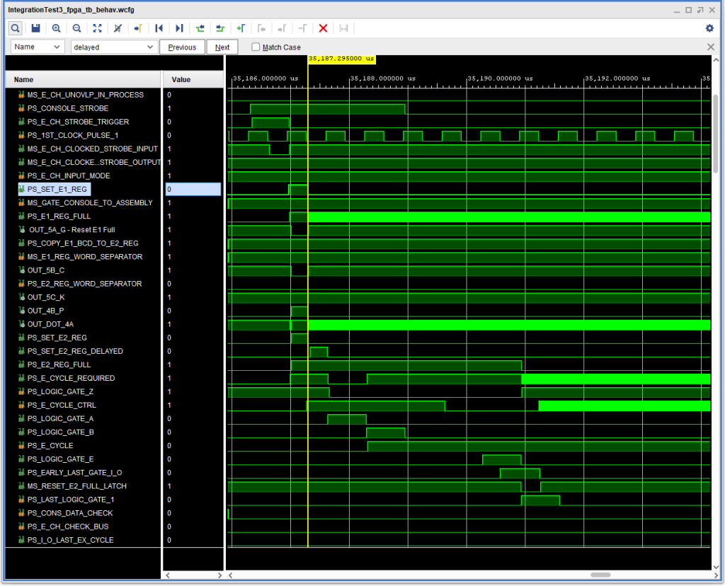
The basic problem was that as I/O was ending, the I CYCLE CTRL signal goes active while E CH UNOVERLAP IN PROCESS is also active.

The problem can be seen in this waveform capture:
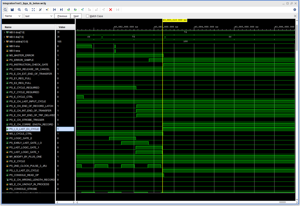
Instruction Check during completion of console input where the number of characters entered is less than or equal to the number of expected characters.

What made this problem a bit more interesting was that this error did not occur if the number of characters entered was more than the available buffer (i.e., from the address specified in the read instruction up to and not including the group mark with a word mark that marks the end of the input buffer:
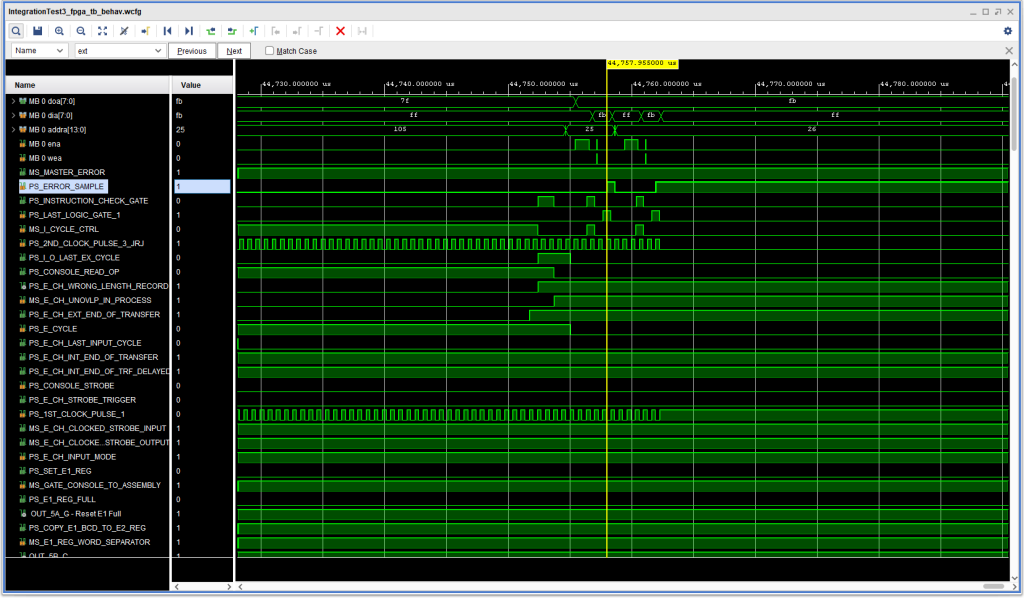
NO Instruction Check during completion of console input where the number of characters entered is greater than the number of expected characters.

I spent quite a few days looking at this and that and trying this and that, without making much headway. And in the process I discovered a couple of interesting errors in the IBM CE documentation for the 1410.

One thing I noticed was that the logic for an Instruction Check that is shown in the IBM 1410 System Fundamentals manual, S223-2589 and is quite simple would not have caused this Instruction Check, and that the logic in the Instruction Logic Diagrams, R23-2936 does have logic that would trigger an error under these circumstances and is more complex. The latter matches (more or less — more on that later) the ALD and triggers this error from either of the bottom two sets of (ILD) AND/OR gates in the lower left hand corner of Figure 58 of the ILD. (In reality, these are implemented using AND/NOR gates – aka And/Or/Invert gates).

The second thing I noticed was that in the I-O sequence diagram on page 43 of the 1411 I/O Operations Manual 223-2692 depicts +S I CYCLE CTRL indeed overlapping +S E CH UNOVERLAP IN PROCESS – in contradiction to what is on the ILDs.

Finally, in comparing the ILD to the ALD I did spot one error in the ILD. In the bottom most And/Or gate on the ILD, there is an OR gate for signals E CH OVERLAP IN PROCESS and I CYC CTRL. In fact, that one is F CH on the ALD (which make more sense).

So, what to do. I had some concern that the change I made earlier to ALD page 12.12.62.1 to inhibit E Cycle Required during Logic Gate A might be a problem, but thought experiments didn’t bear that out. Also, the condition seemed to be benign, in that once the I/O completed, E CH UNOVERLAP IN PROCESS would be de-asserted. Finally, I wondered it this might be another case where the speed of the FPGA logic for multiple layers via LUTs – look up tables – might be causing a race condition.

In the end, I decided on a simple approach. I created a variant of card type DHL, called DHLJ, with an extra direct input to the NOR gate, using otherwise unused pin K. I then fed in the I-O LAST EXEC CYC signal into ALD logic blocks 4E and 4H, which resolved the Instruction Check.

This is shown in the following timing diagram:
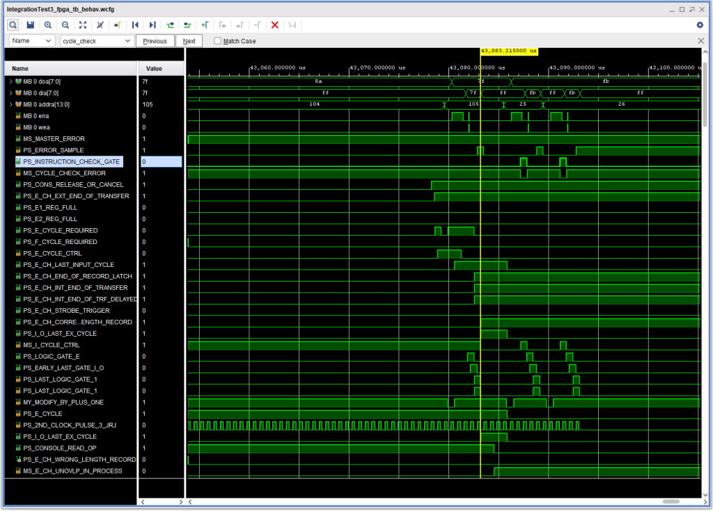
Input Instruction Check fixed by inhibiting an instruction check when IO is finishing up and +S I-O LAST EX CYCLE is active.

This isn’t the most satisfactory thing in the world, but given the contradictory nature of the IBM materials, I didn’t feel like I’d be able to sort it out properly – at least for now. (Also note in the above timing diagram the “notch” in +S E CYCLE REQUIRED during Logic Gate A, caused by the earlier fix.)

With this fix, there are no more problems running the 1410 diagnostic CU01C, nor the 1401 Mode diagnostic M011, including console input.

There is still much to do, including replicating the E Channel fix to ALD 15.41.10.1 into the F channel. After that, I think I will spend some time cleaning up console operations, where there are lots of things to change on the PC Support program software side, as well as some hardware issues, like the improper prompt character during the start of a console Display operation (and other operations as well), and some possible issues during address set and storage load and regen operations.

IBM 1410 FPGA: No. 5 sez: Need More Input

As mentioned in the previous post, during testing of the 1401 compatibility of the IBM 1410 I discovered that console input was not working properly for the machine in either 1410 or 1401 mode. The 1411 CPU would accept the characters, but only the first was entered into storage (if that), and pressing Inquiry Release or Inquiry Cancel did not terminate the I/O operation. After some trial and error signal examination, I discovered that the E1 Register Full latch was “oscillating”, and the cause seemed to be a simultaneous set and reset signals.

In the original hardware, this was unlikely to occur, given multiple layers of logic gates, signal travel times on the backplane wiring, and so on. But in a simulation, or in an FPGA the combinatorial logic signals are implemented using look up tables (LUTs) making instantaneously simultaneous combinatorial signals a likely possibility.

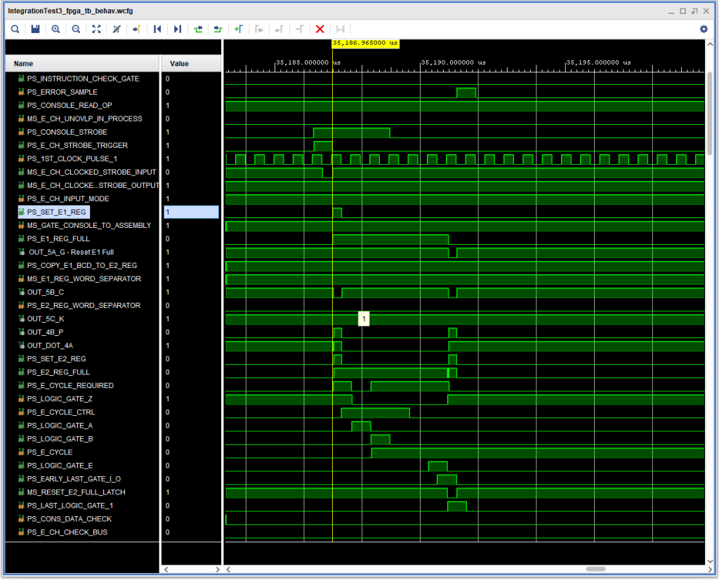
Timing Diagram showing problem with E1 Reg Full being set and reset at the same time, resulting in an unstable latch.
Timing Diagram showing problem with E1 Reg Full being set and reset at the same time.

So, how to prevent that? The first, more or less obvious thing, was to condition one or both of the set and reset signals to give one or the other priority. I found that if I gave the reset signal priority (by inhibiting set when reset was active) that console output was negatively affected, because this change affected both input and output.

However, if I added an inhibit from the set signal to the logic block at 5A, so that set for just input had priority, the problem went away – I could type characters into the console and they were properly entered into memory.

But I also noticed that doing the fix that way I ended up with second pulse of +S SET E2 REG during the cycle. While this didn’t seem to cause any real problems, I was nervous about possible future effects. In addition, it left the E1 FULL signal active for longer than it needed to be.

First attempt to fix E1 Set/Reset Latch problem resulting in duplication of +S SET E2 REG

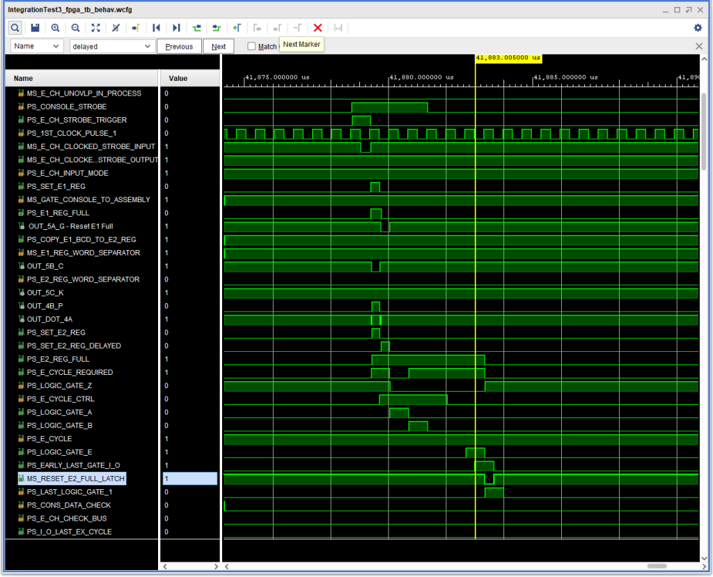
While looking at ALD page 15.62.04.1, which generates signal +S SET E2 REG, I noticed another signal, delayed by 1 IBM 1410 clock pulse, +S SET E2 REG DELAYED. Feeding that into the logic block 5A on ALD page 15.41.10.1 instead of +S SET E2 REG allowed an earlier reset of the E1 REG FULL latch to the time where it really should be happening, and prevented the extra +S SET E2 REG pulse from occurring.

Fix for E1 REG FULL latch problem by using +S SET E2 REG DELAYED

I am a little concerned about the +S E CYCLE REQUIRED being inactive during Logic Gate A, but it doesn’t seem to be causing any problems so far.

However, there is still one remaining issue with console input. If I enter more characters than are allocated in the buffer (terminated by a Group Mark with a Word Mark), the M%T0xxxxxR instruction ends normally. But if I enter fewer characters or the exact number of characters expected, the instruction ends with an Instruction Check, I think because I CYCLE CTRL and E CH UNOVERLAP IN PROCESS are both active at the same time. In the CE instructional text manuals, this check is not present in the logic, however in the ILDs it is present. The question is whether the test should not be implemented the way it is (perhaps by adding some signal to the logic), or if it is just an inopportune appearance of a Error Sample pulse at that time.

IBM 1410 FPGA: We ain’t got no 1401 Overflow anymore?

The last issue that I had running the 1401 diagnostic (aside from Console I/O input working in neither 1410 nor 1401 mode) was “ERR ?3S” in diagnostic M011A, which corresponds to diagnostic location 07032 (the routine actually starts at location 06980). This is test RN111, the very last test in the diagnostic.

The diagnostic comment block says it all:

RN111
TURN ON OVFVLW IND WITH ADD INSTR
EXECUTE BR INSTR WITH UNITS PSN OF
A ADDR CONTAINING Z
TEST FOR OVLW IND STILL ON

Trouble was, the overflow indicator was indeed off after executing the branch instruction at location 7016 (which branches to location 7899, which was set up to just branch right back to location 7020.) What is so special about the “Z”? Well, it turns out the “Z” is the d-character for a B(I)Z instruction – branch on overflow (a sample of which is at location 7027). But why should that ever be in the Op Modifier register for an unconditional branch instruction that has no “d” character?

Well, it turns out that the 1401 mode instruction readout often places a character from the address into the Op Modifier register, as noted in the IBM 1401-1410 Compatibility CE Instructional Manual, Figure 3B on page 9.

There were a few possibilities for this problem, and a few possible cures for this. In the end, some simulation runs demonstrated that the reset occurred because “Z” was indeed still in the Op Modifier register when the unconditional branch was set up.

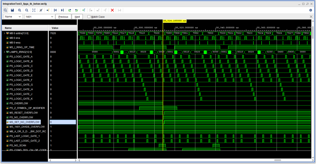
Simulation trace showing the Overflow indicator being reset during readout of a Branch Unconditional instruction with "Z" as the last character of the address.
Simulation trace showing the Overflow indicator being reset during readout of a Branch Unconditional instruction with “Z” as the last character of the address.

There were several possible cures that might have fixed this, focused on the fact that in a normal B(I)d conditional branch the d character is read out later in the I cycle – so maybe one could reset the Op Modifier register after the address was read out and the following character had a word mark – indicating that the branch had not “d” character at all. But in thinking about it I wondered why this very specific test was in the diagnostic – and as the last test, which maybe meant this was an issue that was uncovered in the field (and perhaps only on machines with the Accelerator special feature).

The reset of the Op Modifier register is controlled on ALD 15.38.04.1. Interestingly, a very relevant signal, +S CHAR TEST BRANCH OP CODE that this page says originates on page 13.13.05.1, does not show up on page 15.38.04.1 as a destination. I had had to “add” that signal into the signal list when I came to page 15.38.04.1 when I entered the data for that page into the database. Perhaps more interestingly, the Instructional Logic Diagram for this ALD, part of ILD Figure 26, shows the signal as instead being +S 1401 COND TEST OP CODE , and is designed to reset the Op Modifier register when:

  • +S 1401 COND TEST OP CODE is active AND
  • In 1401 Mode AND
  • The B Channel has a WM Bit (i.e., end of the instruction) AND
  • Logic Gate D AND
  • I Ring 8 Time

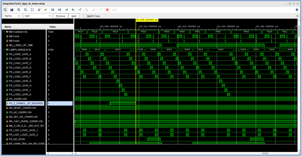
Well gee whiz… this was exactly the kind of signal I was looking for to fix this problem. So, to fix it, all I did was change +S CHAR TEST BRANCH OP CODE on the ALD to the one the ILD specified, +S 1401 COND TEST OP CODE, and the problem was cured, with no side effects causing other problems.

Simulation trace showing the reset of the Op Modifier register during I8 time during readout of an unconditional branch instruction.

So this was presumably a case of either a) a mismatch between a page denoting it is for the ACC feature (15.38.04.1) and the source page of 13.13.05.1 which does not call out the ACC feature, or, perhaps, page 15.38.04.1 being “down level” – not having a necessary ECO t fix this. When I did the change, I set up an “ECO” JRJ005 in the database.

With this, the 1401 diagnostic M011A runs to completion without errors, as does the 1410 CPU diagnostic CU01.

During this testing, however, I discovered an issue affecting both 1410 and 1401 mode: Console I/O Input does not work – the characters don’t seem to make it into “core”, and when Inquiry Release is pressed, the I/O operation does not complete. This could be something as simple as a support console software bug or, more likely, an issue in the interface between the 1415 console emulation VHDL and the 1411 CPU Channel, since 1415 Console Input during console control operations (setting addresses, memory data, etc. all seem to work mostly OK). Time will tell.

IBM 1410 FPGA: S’more SAR Instruction Issues

So, not the yummy treats, but a new problem that showed up with the SAR instruction.

The fix to ERR 60J was pretty easy. That was a gate for feature S10 – a 10K 1410 that needed removing (and its output replaced by a logic ‘1’) on page 14.30.05.1. QED.

However, after fixing that, I then experienced an error near another Store A Address (SAR) instruction, at (just before) location 8624, exhibiting A Channel, Assembly Channel and Address Exit validity checks, with garbage in the B Address Register. However, when I ran the same instructions in the same place in the address space (but with memory otherwise all blanks) it seemed to work just fine. How could this be?

The first blind alley was either that the print chain used for the diagnostic listing printed the 1410 characters “?” and “!” as “&” and “-” respectively, or there was a bug in the listing version that was fixed on tape. So much for that hypothesis.

To figure this out it would be best if I could get it to fail under simulation (There is a scoping capability in the FPGA as well – but not as quick and easy to use.) As mentioned above, during initial testing for this problem, I just loaded the relevant instructions into the appropriate memory locations with memory from 10K up to 40K being blank characters and the failure did not occur. Further more, during testing I discovered that if I had only loaded the first 10K of the 1410 1401 mode diagnostic, M011, as the listing only went up to just under 9K, this problem also did not occur, and the only error ?3S (translated into address 07032). However, that diagnostic is ordinarily loaded from the 1410 diagnostic program TC50, and when I used the image that I have that goes up to 40K, all heck broke loose with the error noted above. I then changed my memory initialization to all ‘9’ characters aside from the instructions under test and was able to reproduce the issue under simulation.

This led me to an initial suspicion that something must be causing more than one B character register from “core” to read out simultaneously. Only one is supposed to read out at a time – and their outputs are OR’d together. If more than one read out at the same time, the results would be problematic. But how was this occuring?

After many simulation runs looking at various signals and what might be going on, I finally hit upon this one.

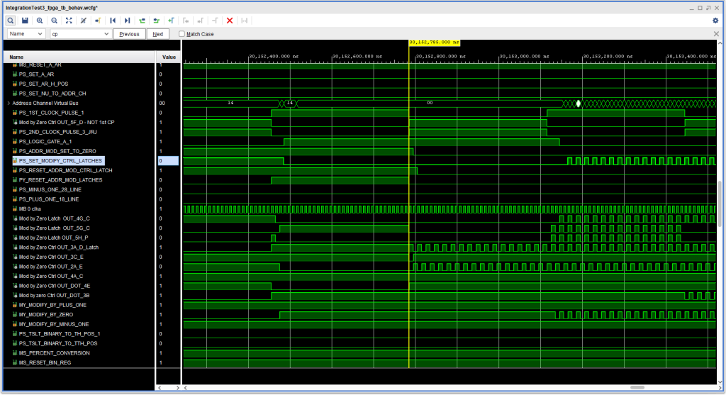
IBM 1410 1401 SAR Instruction Set / Reset Race with '9's in 10K-30K
IBM 1410 1401 SAR Instruction Set / Reset Race with ‘9’s in 10K-40K

Looking at the timing diagram one can see signal -Y MODIFY BY ZERO essentially “oscillating” starting shortly after 30.153 milliseconds. That in turn caused the Ten Thousands position to change quickly, resulting in the issues as that position is used to select among the B character registers from memory. That latch “oscillation” then in turn set up problems all over the place, particularly in the Address Channel.

Looking again at the same timing diagram, one might notice that +S ADDR MOD SET TO ZERO and +S RESET ADDR MOD CTRL LATCH are both active when +S RESET ADDR MOD LATCHES becomes inactive. Those two signals both impact the Modify By Zero CTRL latch at blocks 3A and 2A of ALD page 14.30.09.1, resulting in the signals trying to simultaneously set and reset that latch – a pair of cross connected NAND gates – a typical R/S latch. This is a big nono.

In my ALD page generation, these latches are recognized, and “D” flip flops are added after each gate involved. So instead of being undefined, in this kind of situation a kind of “oscillation” is set up at about 1/2 the FPGA clock speed of 100MHz (which is also the memory clock signal “MB 0 clka” in the diagram).

The general approach I took to fixing this was to either a) prevent a set during a time when the reset signal was present or b) prevent a reset during a time when the set signal was present.

To try the first approach, I added the +S ADDR MOD SET TO ZERO signal as an input to get logic block at 3C on page 14.30.09.1. This was done directly in the VHDL – much quicker than puzzling out where to find/fudge a logic block to add to the equation and test – especially if, as in this case, the fix doesn’t work. So, apparently this situation really needed to do a Modify Address by Zero operation (which it did: this, like the previous problem, occurred while copying the contents of the A Address Register to the B Address Register.)

So, then I went to the other approach, (undoing the first one), which was to add the +S ADDR MOD SET TO ZERO signal in so as to inhibit a reset while it was active. That indeed fixed the problem, and the change to the ALD was very easy: all I had to do was add the +S ADDR MOD SET TO ZERO signal into the existing “wired OR” at ALD coordinate 4E, as “ECO” JRJ004.

As for the original 1410 implementation, this could easily be another case where the fast FPGA logic causes an issue that never cropped up in the real hardware.

After doing this, the diagnostic worked OK except for the ERR ?3S. (I have not yet tried the manual part of M011 – testing the sense switches, etc.).

Getting close…