
The last 12 months I have been pretty busy working on my 1410 in FPGA project, and there is now more to share, though I have not done much actual work since February – been too busy playing with other “toys”. 8D
First, I finished working through all of the IBM 1410 and IBM 1415 Automated Logic Diagrams – generating VHDL and testing the results with test benches. [Note that this includes the built-in 1401 compatibility mode, activated at the flip of a switch.] That took most of 2020.
So, the CPU generation in VHDL is now more or less complete, and I added a hand coded memory module for memory, as core is kind of hard to find on an FPGA development board. 😉 I am currently using a Digilent Nexys 4, but I think it might have even fit on a Nexys 2 – there is plenty of room to spare, and there isn’t anything in the VHDL aside from, maybe, the memory implementation (though even that is pretty generic VHDL).
With this the CPU runs, at the very least, Unconditional branch (Jump), Halt, NOP and Set Word Mark instructions seemingly correctly – I haven’t tried any others. Somewhat surprisingly, aside from issues with the hand coded VHDL in triggers and the need to communicate pins tied to logic one or zero, the auto-generated VHDL works untouched.
I have updated the github repository for the C# database application that generates the VHDL from time to time (and which includes the complete database) at http://github.com/cube1us/IBM1410SMS
There is now a *new* repository, http://github.com/cube1us/IBM1410FPGA which holds the generated VHDL, some hand coded VHDL modules for certain SMS cards (typically for triggers, for example), the console and test benches I used along the way, and VHDL “Integration Tests” which are designed to be loaded onto the board – the current one being IntegrationTest3.
There will be, eventually, a third repository which will contain the C# code that “hosts” the IBM 1410 console and peripherals, communicating with the FPGA over a high speed serial over USB connection. I figured out that this should allow me to emulate peripherals without having to resort to sending data over Ethernet, SPI, I2C or the like. I have just started that, so it really isn’t at a point that there is much to share.
Once I have a console working (which will require a re-do of the console VHDL implementation, which right now communicates in ASCII, but should probably be using BCD), I should be able to pre-load into memory some of the CPU diagnostics, by loading a diagnostic routine into either my 1410 simulator (http://github.com/cube1us/1410), or Richard Cornwell’s emulator in SimH and then taking a snapshot of “core” to pre-load into the FPGA. At that point I expect I will be able to test the CPU pretty thoroughly. I hope and expect that will happen this year sometime.
Unfortunately, I do not have the ALDs (Automated Logic Diagrams) for the IBM 1414 I/O Synchronizers, but I do have the Instruction Logic Diagrams which should allow me to code VHDL to emulate card, tape and maybe eventually even disk functions, so those might take a while.
Category: Computers
Posts relating to computers
IDE to SATA SSD Conversion: Adventures with a Pentium II and 1.33 GHz AMD Athlon
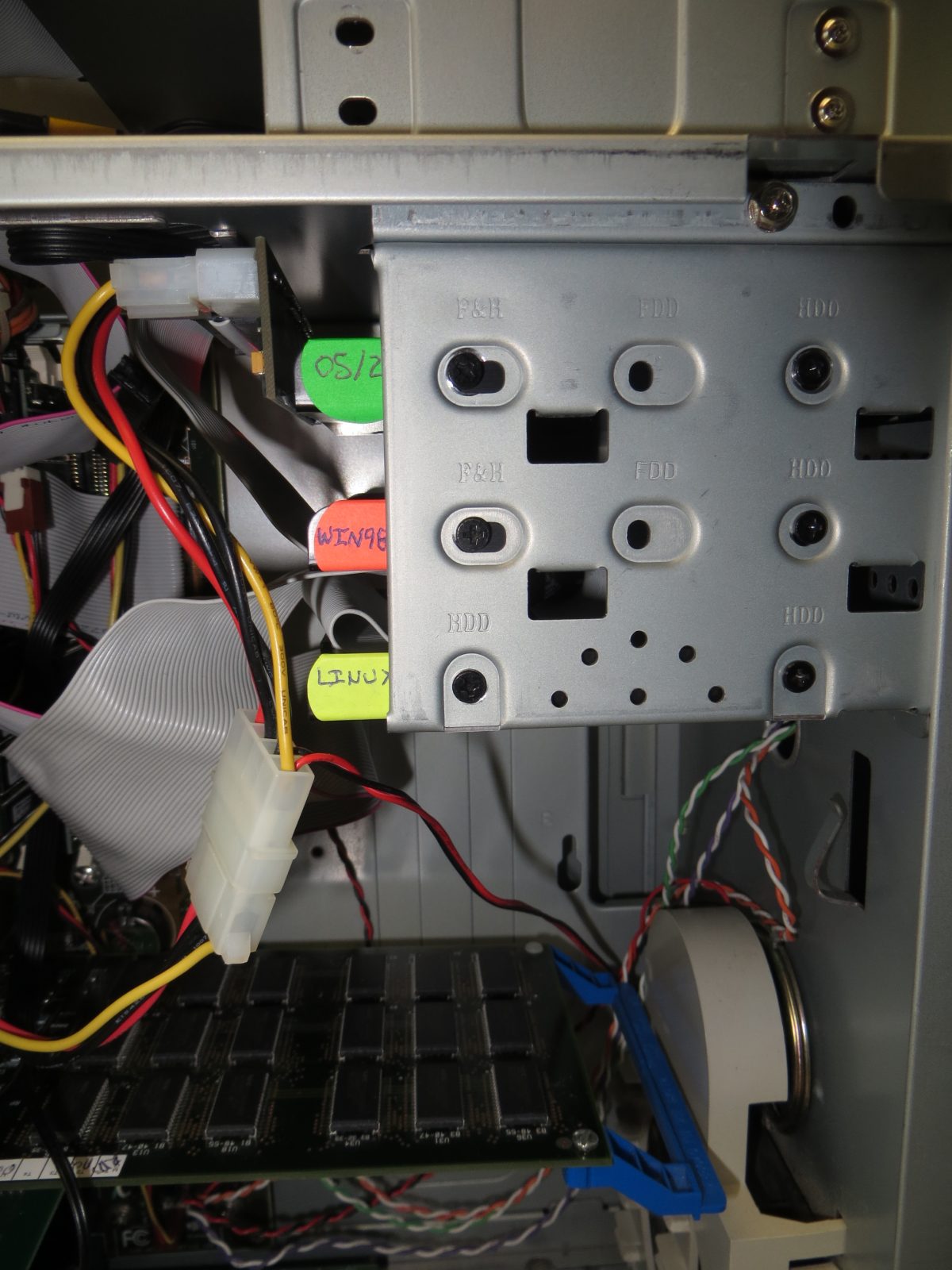
In early 2021, I converted the hard drives in my Pentium II computer which hosts my P/390E IBM mainframe processor card, which I call “Floppy Copy“. This machine boasts three different operating systems. Two are in support of its primary mission for copying floppies: Linux to host my Catweasel board (which may not see much future use, now that I have a Greaseweazle board), and Windows 98 for copying floppies using tools like IMD. It also has OS/2, in support of the P/390 board.
First some background: OS/2 had always acted a little wonky: I did the partitioning under Linux because OS/2 didn’t like to partition the 200GB drive. And then, having partitions of 2GB, 57GB, 57GB and 57GB, running OS/2 chkdsk on the last two 57GB partitions would sometimes clobber the first 57GB partition, for reasons I never understood – until I undertook this migration. (I still don’t quite understand why it never managed to clobber the 2GB FAT partition!)
So, off to Amazon I went, purchasing IDE to SATA adapters. The two from Startech and Kingwin worked fine. One from Sinloon worked, and the other did not work at all. In addition, I found, strangely, that the adapters would work with a 240GB drive, but not a 120GB drive. WTH?
So, then I went looking to see if the BIOS might be involved, and I found a BIOS update from Aug-17-1999 to Sep-09-2000. That cured the 120 GB problem. But then, in testing, I ran into the same kinds of issues on the 240GB drive I had seen on hard drives, with corruption after running OS/2 chkdsk.
Well, it turns out that this particular motherboard, a Chaintech 6BTM, has Ultra DMA-33 IDE ports – and only supports drives up to 137GB. Ahhh, so that was the problem.
I wanted to give OS/2 (and the P/390E) as much space as possible, so it got one 120GB drive. I tried and tried to move the drive partitions for Windows 98 and Linux over to a shared 120GB drive, but without success. The minute I created a second primary partition for Linux, Windows 98 would no longer boot. So, I simply imaged Windows 98 as is to a 120GB SSD (using only a fraction if it), OS/2 to a 120GB SSD and Linux to a 240GB SSD – because I already had it, having purchased it from before I learned about the 137GB limit.

Only one of the three adapters I had supported IDE master/slave. The other two had to be alone on their cable. I am using one of those two (Kingwin) permanently.
Having gotten things tested, I went about testing the IDE to SATA adapters one at a time in order to write reviews. While testing the Kingwin adapter, though, I decided to plug it in with power on. Unfortunately I had the power connector upside down, and as soon as it touched, the computer dropped power. Worse, I could not then power it on at all — completely dead. Ohhhh nooooooooo!!!
After unplugging the power cord for a couple of minutes, I could at least try and turn it on, but it would not start up – no beep, no nothing. Fearing the worst, I tested the power supply voltages – all fine. Ohhhhhh noooooooo!!!
After 10 minutes of panic, I started testing cards from that machine in a reasonably close relative, my AMD Athlon machine with an ASUS A7M266 mother board. Video card: good. IBM P390/E even passed its diagnostics. (Whew). So then I pulled all the cards out of the Pentium II as well as the IDE to SATA adapter I had been messing with at the time of the infraction, and the machine came to life!
I put all the cards in one by one, and stopped at the POST test. All good. Then, just for giggles, I hooked up that last IDE to SATA adapter – dead in the water, apparently fried. Embarrassing: I fried an adapter. The good news: it costs less than $10. Glad I purchased four of them. (I kept the Startech out in reserve because it is the only one of the four which worked and can be set for Master or Slave.)
Having discovered that the P390/E was happy in the AMD with the A7M266 motherboard, and that the motherboard has OS/2 support as well, so in May 2021 I migrated the P/390E to the AMD machine, and upgraded to OS/2 Warp 4.52, so now I have support for the full 240GB SSD.
IBM 1410 FPGA: Console Output
Getting console output was going to require writing some VHDL of my own – I don’t have an actual IBM I/O Selectric available! I started out by reading through the material in the IBM 1415 Console CE Instruction manual (S223-2648) to design some finite state machines (FSM) to stand in for the console cams and feedback contacts.
The I/O Selectric uses cam contacts to control the timing of things like when the type ball tilt and rotate has completed, when shifts have completed, when spaces and backspaces have completed and when a carriage return has completed. It uses additional feedback contacts to indicate the parity of the received character, whether the keyboard is locked and the current shift state (upper or lower case).
To save time, particularly during simulation, I sped those timings up by a factor of 100. Mostly this just involved the console implementation module itself, via a VHDL generic parameter, but I also had to adjust the single shot on ALD 45.50.01.1 as well.
The Selectric also uses a set of solenoids to initiate actions such as printing a character, locking/unlocking the keyboard, spacing and backspacing, carriage return and shifting from/to upper and lower case.
After writing some simple state machines for the cam timing, I enabled the normal stop print-out in the CPU via a test bench signal, and then used simple VHDL with “wait” statements to check for the outputs and provide the input signals required by the CPU in order to test my understanding under simulation.
The first thing I came across was a latch on page 45.50.15.1 that did not have a reset. In real world hardware this can work because (unless it enters a meta-stable state on power up) it will be in one state or the other. However, under simulation that does not work – it ends up as an undefined signal – so I added a Program Reset signal to the latch at location 4A on that page to compensate.
The next thing I saw in the traces – which I hadn’t expected, but probably should have – was activation of the carriage return solenoid so I had to add the FSM for that. (Note: The I/O Selectric implements a carriage return by returning the type ball to the home position and initiating a paper (line) feed operation).
This was then followed by an “S” character – and the fun began. The interface feedback signals from the Selectric are full of names that end NC or NO (normally closed, normally open). Now one might expect that these refer to the state of those signals at idle, but the cam contacts aside, that quickly got pretty confusing – more so because most of these signals (except those that drive the solenoids) are active low. In addition, the keyboard lock signal is -W on the CPU diagrams, but +W on the 1415 Console Printer contact diagram page 40.30.01.0, and a couple of the feedback signals from the Selectric to the CPU are marked as -B level on the ALD page — but are actually -V level, as can be determined from page 40.30.01.1 as well.
Eventually I came to the realization that the best way of handling the NC vs. NO +/- confusion was to more or less ignore it, and instead use the signal name and level to determine what state a given signal ought to be in at a given time. That helped a lot. Once I got ordinary characters working right, I proceeded to code the state machines for space/backspace, and shifts.
Shifts were a little problematic at first, because the CPU drops the solenoid drive the instant it sees the feedback signal from the Selectric – which didn’t give me a clock cycle to save the new shift state.
Once I got that working under simulation, I turned my attention to getting that I/O from the Selectric to a PC for display. A few months back I had looked into using a MicroBlaze soft CPU to do that, but looking at how my Digilent Nexys 4 USB to PC connection works, I discovered I can run successfully at speeds of at least 115,200 bits/second, which should be plenty enough to run a simple flag bit/type protocol for not only console output, but also switch inputs, printer output, card input, tape I/O and disk I/O – perhaps adding a silo or two for lower priority devices. This is a huge simplification over what I had been thinking would be necessary.
But at this point there was also a little bit of extra work required. initially I had written the VHDL to use character output for the UART, but I subsequently discovered that VHDL doesn’t have a consistently synthesizable way to convert from character to std_logic_vector, so now that type-ball characters are specified as std_logic_vector bit strings, instead of ASCII characters – which is probably better in the long run, anyway. Mostly I am using the same encoding I used from the IBM 1410 simulator software, which in turn was derived from Joseph Newcomers IBM 1401 emulation software.
Once I had tested the UART VHDL, found at Nandland, I put together a test to combine that with the CPU and generate a bitstream for the FPGA. I had two small problems in the process – trivial ones, really. The first was that I keep forgetting to wire signal “+P SPECIAL +12V POWER FOR OSC” (which then feeds “+P SPECIAL +12V FOR REL DRIVERS”) to logic ONE. The second issue was that while most of the buttons on the Digilent Nexys4 are active high, the Soft CPU reset button – which I feed to the 1410 CPU Computer Reset signal is active LOW – wasted an entire day on that one. 8(.
One I did that, I obtained the following result: A printout of:
S 00009 00007 00007 .c … _ _
This is exactly the expected result (one which I had already observed in simulation). The “c” is a 1410 blank (different from the console space operation), and will print as a “b” using a PC-side application. Also, the three periods after that, which are the contents of the A Data Register, B Channel and Assembly Channel, have wordmarks – which you cannot see in the PuTTY output because they get backspaced over. Finally, the last two characters, the channel unit select and unit number registers for Channel 1 are wiped out by the backspace/underscore combination that occurs because they seem to be uninitialized, and therefore have bad parity.
Next on the list will be cleaning up the latches in the VHDL code which are currently tracking upper/lower case, tilt, rotate, space/backspace, and the character to be sent to the UART, and maybe a couple of more, as well as working on the PC side console application – starting with designing the protocol I will use for PC / IBM 1410 communication.
IBM 1410 FPGA Testing, and Memory
“There you go again”
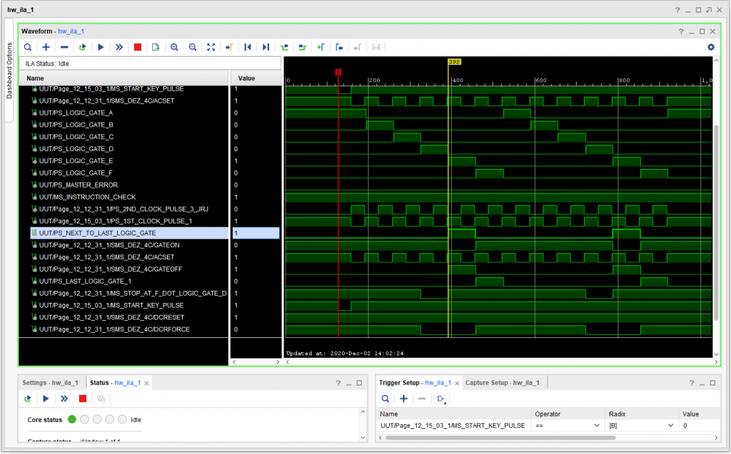
What with the Thanksgiving holiday and all (even though it was spent at home, ’cause 2020), it took several days to ferret out the issue where simulation of a power on reset followed by START worked, but on the FPGA that failed. Of course it was bound to be an issue with triggers. However, I used the Integrated Logic Analyzer (ILA) to confirm that issue before I changed anything. Sure enough, card type DEZ needed the same adjustments as DEY: I changed it so that the transition of the AC SET input was required to occur after the transition of GATE ON / GATE OFF. At the same time, I moved all of that logic inside the FPGA clock transition section, to make it synchronous with the FPGA clock. That fixed the issue, which occurred on page 12.12.31.1
So now, after I load the FPGA, all I need do is press START and I see the correct waveform. (Also note that the transition of the output to ON (NEXT TO LAST LOGIC GATE) immediate turns off GATE ON – because that is exactly how it is wired. So first we see -S (active low) STOP AT F . LOGIC GATE D at about 320 into the trace. Note that GATE ON is already present, however, the trigger is held off by the “DCRFORCE” input coming from block 3B until STOP AT F . LOGIC GATE D goes true. Next, we see CLOCK PULSE 2 appear (but it gets inverted before it us used for ACSET, so it essentially matches CLOCK PULSE 1) at 389 on the diagram. Then at 392, the trigger sets, NEXT TO LAST LOGIC GATE goes true, and GATE ON is removed.
Decoding Memory Addresses
The IBM 1410 storage address register (STAR) is a five position two-out-of-five code register. However, it is not used altogether to select an address. On a read, all of the 10,000 position core memory segments are read, in parallel, each to its own B data register position. So, for a 40K machine, it has 4 B data registers, for 0-9999, 10000-19999, 20000-29999 and 30000-39999. On a read, the ten thousands position of the memory address is used to select one of the B data registers to gate onto the B Channel. During the write portion of a memory cycle (to change memory, or to regenerate memory if only a read is required), the ten thousands position is used to decide which B data register to update, if any, before the write portion of the memory cycle. The other B data registers retain their original contents from the read cycle.
At present, rather than simulating the full core plane of the IBM 1410, I chose to implement memory, for now, using a binary address and (probably) an array of 10K FPGA Block RAM segments. This means that the binary addressed RAM for the FPGA IBM 1410 uses a 14 bit address (to cover 0-9999), with memory arranged in the same 10K sections.
The inputs into this decoder are the -Y MEM AR UP/TP/HP/THP signals, which are in two-out-of-five code. The output from the decoder is a 14 bit binary address, 0 – 9999. This was implemented “brute force” by decoding each of the positions to the appropriate binary number, so the UP decodes to 0 – 9 in a 14 bit binary number, the TP decode to 00 – 90 (by tens) in a 14 bit binary number, and so on. Then the four binary numbers are simply added together in the VHDL – leaving the implementation of the adder for the tool chain to figure out.
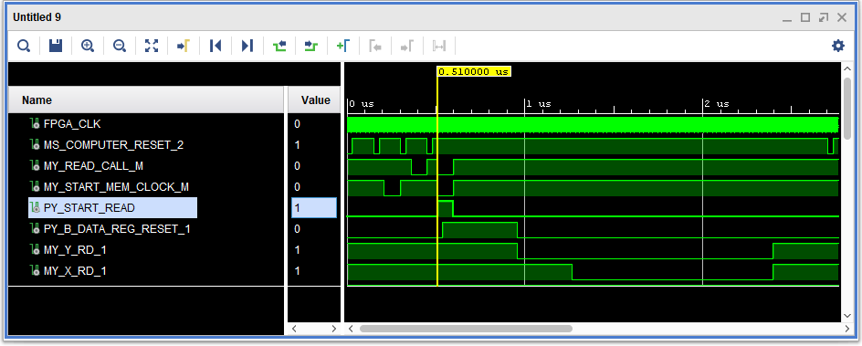
Memory – and a Startup Issue
Next I created a simple set of Block RAM modules (BRAM) along with a VHDL wrapper for the 40K main core unit, accepting the aforementioned addresses in 2 out of 5 code, the Ten Thousands position (so that eventually it can tell if it is the 40K main core or the 60K Z Frame core), inhibit signals, and output sense signals. In order to more easily generate the necessary BRAM enable and write enable signals, I also brought out the MY_X_RD_1 and MY_X_WR_1 signals.
After some fussing I got my BRAM module working under simulation, but ran into an odd problem where during startup the system would overwrite location 00001 with garbage (and presumably 10001, 20001 and 30001 as well) because the system was left in Logic Gate B (LGB) state during the power on reset that then proceeding through a memory cycle once the power on reset was complete triggering the computer reset- thereby writing those locations with uninitialized garbage. (Computer reset will finish a cycle if it is encountered mid cycle to avoid corrupting core.)
I temporarily disabled memory writes, and then found I could successfully execute my halt instruction (WM/. WM/. in locations 1 and 2) under simulation AND on the FPGA.
The startup issue was interesting. I had supposed that the power on reset signal issued on ALD page 12.65.01.1 would start OFF, come ON during the power on reset, and then turn OFF again. However, that was having the undesirable effect of letting the system progress from LGA to LGB during the power on reset as mentioned above. Some study of the aforementioned ALD, along with the IBM 1415 console manual (the power on switch is located there) made me realize I had misunderstood.
That power on reset signal is asserted during power on to keep the system in a reset state (and thus in LGA) for an RC constant of about 500ms. Then, after that, the signal goes to logic 0, triggering the one-shot at block 2D to do a computer reset. At that point, the machine is in LGA, and the computer reset will leave it there.
Since I already have a system initialization VHDL process in the FPGA VHDL logic, it was easy to manage the power on reset signal there – indeed, the two may eventually become one, as they both have the same purpose of getting some stuff set up before letting the IBM 1410 CPU start.
This tested OK under both simulation and on the FPGA, though I have not yet verified that the FPGA is actually writing the contents back into the BRAM.
Next up: testing write by setting a wordmark somewhere (to verify read/write), and then halting, and a simple loop – both of which should be possible with my current VHDL by just changing the RAM initial values.
Update: The instructions sequence, starting at location 1, of setting a word mark at location 8 (which takes locations 1 through 6), a NOP instruction (reading out the set word mark instruction needs a wordmark on the character after) and then a period (halt without the word mark) behaves correctly. Wohoo! I have something of a CPU.
Next up: starting work on the console.
IBM 1410 FPGA Continued – Simulation and Initial FPGA Programming
Having completed the pass through the ALDs, the next thing I undertook was some cleanup work. The goal was to be able to generate an HDL “group” that contained ALL of the usable HDL pages.
The first step of that was to mark pages I didn’t want as no HDL generation – a relatively recent addition to the application. Then I went through and found all of the switches, and regenerated the affected pages to use update code that used notations in what is ordinarily the signal level fields of the ALD logic blocks associated with the switches (but show up as thinks like DK 2 – meaning switch deck two of a multi-layer rotary switch). I also had to fix up the associated test benches and groups to use the new signal names.
Then I took a shot at generating the whole shebang. I ran into three issues. There were a couple of pages I had skipped that had to do with auto-restart. Dealing with those was simply a matter of marking them to not generate. Next, I ran into an issue with page 13.72.06.1 – which turned out to be a missing page having to do with compute disable cycles for systems with “fast” file (disk) systems. Finally, the ALDs had several cases where the same IBM 1415 console lamp location was specified. I separated them arbitrarily – I don’t seem to have any specific information to help me decide.
Simulation Begins
With those fixes I was able to begin simulation. At first the power on reset wasn’t working right – the 20ms single shot on page 12.65.01.1 wasn’t triggering. This is really a simulation issue, I think – putting in a 30ns wait at the beginning of the simulation dealt with that.
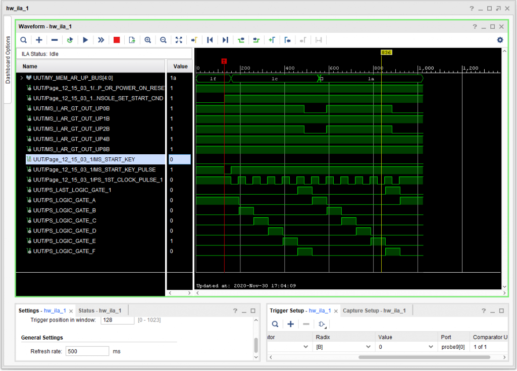
The next issue was that after the reset, pressing the start key did not start the clock – the STOP LATCH stayed on. That in turn kept the clock from starting (ILD Figure 1). That in turn led to noticing that there was no START KEY PULSE when the start key was pressed in the simulation.
Part of the issue was tracked down to the fact that I don’t yet have a console printer emulation in place, and the console contact signals were inconsistent (both C1 and C2 normally closed and normally open signals were false), so I “fudged” it so the cam contact signals would indicate it was not in a cycle. That helped – and was the sort of thing I expect might need attention.
The next issue with the START KEY PULSE signal was that the CONS STOP PRINT COMPLETE signal was 0 – as though it was in the middle of a console stop print out. That was traced down to the Console STARTPRINT switch (page 44.10.01.1) which is unusual in that its N output (usually reserved for an active HIGH signal) is active LOW in this instance. That got me to the point where the START KEY PULSE appeared, and the machine went from Logic Gate B (perhaps it should have been at A?) through Logic Gate E, and which point Master Error was asserted and things stopped.
The error lamps were multitudinous, but the lamp that was first in line in the time line was the B Register Reset Error. The B register gets the contents from memory, and if it does not reset before then, that is an error (otherwise it might return the previous character, or some combination of the previous character and the current one).
Have I ….
By now, if you have been following along, you know what comes next. Yup. Triggers. In particular, card type DEY, used for generating the clock pulses and also for the logic clock (A, B, C, D, ….). Based on the waveforms I saw in the System Fundamentals manual, I had supposed that the AC input signals for set and reset would remain at logic zero until the gate had been turned on, and then pulsed. However, that turned out to be wrong, and it caused the system to advance into Logic Gate B immediate after reset, which caused the missing reset of the B register, among other things. What the system actually does is that the AC Set signal may already be at logic one when the gate on signal comes along – but since the AC Set signal is capacitively coupled, in that case the AC Set does NOT trigger the trigger. That does not happen until, while the gate is on, the AC Set signal transitions from zero to one.
The CPU Executes Its First Instruction
Upon fixing that, a whole bunch of stuff worked. Upon power up restart, the memory address register – the MAR – and the IAR – are already set to 1. So when START is pressed, that is the character read from storage. The instruction I am force feeding to it is the HALT instruction. Then the IAR gets incremented by 1, loaded into the MAR and the following character is read out (and, since I am force feeding it, the character is exactly the same). Since it has a word mark (WM), the system knows that this is a plain halt, and, lo and behold, the system halts.
This success, though, means that I have to go back and test (though not regenerate) all of the pages that use card type SMS_DEY. They should all be fine.
The IBM 1410 executes its first halt instruction
Well, actually, not all of the SMS_DEY usages were fine – there were four test benches with issues. In each case the AC Set or AC Reset signal was changed simultaneously with a collector pull off signal (DCRFORCE in the VHDL) which caused problems given how I coded SMS_DEY.vhdl. Adding a slight delay between the two (which is realistic) fixed the test benches.
Try and Fit onto the FPGA
With that, I made a couple of tweaks to a copy of the Integration2_tb.vhdl to become Integration2_fpga.vhdl and tried to synthesize it. There were a few issues:
- A couple of signals had no drivers because they did not appear as outputs from the sheet: -S F CH FILE OP is used on 12.12.67.1, ostensibly coming from 13.74.04.1 . 13.74.04.1 has the latter ECO (251849 vs. 251824). Also, the card location chart on page 12.12.67.1 does not show the gates that appear on the ALD. For now, I changed 12.12.67.1 to use signal -S FILE OP instead, and changed 13.74.01.1 to output that signal to 12.12.67.1
- Similarly, on the same two pages, 13.47.01.1 outputs -S FILE OP.D CY.EXTENSION but this got mangled into -S FILE OP.DLY.EXTENSION on page 12.12.67.1. It goes to the same gate as #2 above, so it may turn out to be bogus.
- A signal +S BLOCK USE A CH WM is used on page 15.49.02.1, ostensibly originating from page 15.41.12.1. It does not originate there (or anywhere else). Here I changed the signal to “LOGIC ONE” on the destination page, and removed it from the origin page (which has the later ECO, at 253469 vs.251829).
Fixing numbers 2 through 4 was easy, if tedious – I also regenerated and ran the associated test benches. For a little while I thought #1 was just a matter of Vivado not recognizing the my signal named FPGA_CLK was a clock, but found it was indeed recognized. So I dropped that for easier prey…
There were a bunch of references in the Vivado synthesis log complaining about unconnected signal “GROUND”. This was because it appears as an input to sheets – most of them using it for capacitor input, or, in once case, a switch input that the generated HDL ignores in both cases. So, I changed the app to ignore that signal name, as it does with “LOGIC ONE” and “LOGIC ZERO”. Some of the triggers map a signal named GROUND to an *output* so that they can use it as a logic one internally – those I have left — for now. Interestingly, there were two more pages that had this issue that Vivado did NOT call out with a warning – but then failed when I regenerated IntegrationTest2.
The rest of the unconnected inputs I ignored for now – mostly they are cases where a bit vector is input to a page that does not use all the bits. Heck, that really should not be issuing a warning!
Next up was InvShiftRegister.vhdl. The way I had done the shift, one bit was “undefined” for a while – or conceivably could be. I changed the assignment and tested the affected pages again (39.10.01.1, 02.1, 03.1). No page HDL changes required for that. But what was weird was that this exact same assignment is used in ShiftRegister.vhdl, but there it did not generate the warning – but was not called out (see the discussion regarding GROUND, above, where the same kind of thing occurred).
Loop “D” Loops
Another issue that cropped up during synthesis, and became roadblocks when I tried to generate the bitstream for the FPGA involved a couple of apparent combinatorial loops. The application prevents those from being an issue on a single page, but there is no check across pages. Two such loops showed up, one involving +S CONSOLE PRINTER NOT BUSY and the other involving the A Channel WM bit.
It took me a couple of days to learn how to get the tooling to leave enough information in during synthesis so that I could see the problem. Setting the Xilinx Vivado “-flatten_hierarchy” to “none” made things much easier.
The console issue was easy to fix: I just manually inserted a “D” flip flop on page 45.50.08.1. The A Channel one was harder. The first time I looked at the schematic +S A CH NOT WM BIT was in the loop, so I put a “D” flip flop on that signal on page 15.39.08.1. But then the issue moved to +S CH WM BIT, so I put a second flip flop there. But then the issue moved again, this time to +B A CH WM BIT. Looking at the page I quickly saw that these were all fed from the logic block at 4D, so I took out the other two flip flops and put one at the output of block 4D, which cured the problem, both during synthesis and when generating the bitstream.
With normal settings, the design takes up 2858 LUT (look up table) cells and 1628 flip flops. With flatten_hierarcy set to non, it takes up 4001 LUTs and 1805 flip flops (two of which are the ones I added to fix the loops).
Doing some “greps” on the source, I found I had 1200 D flip flops that I had inserted (generated for on-page combinatorial loops — almost all latches), about 128 triggers, not counting the registers needed for implementing one-shots and delays, so the flip flop of 1807 count seems about right.
At one point the flip flop count had been as high as 2046 with a smaller LUT count, but while looking for the combinatorial loop issue I made a change to the VHDL for trigger card type DEY to bring what it thinks of as a DC Set or Reset into the section edge triggered by the 100MHz FPGA clock which actually made things smaller.
The FPGA on the Digilent Nexys 4 is an Artix 7 XCA100T, which can has 15,850 slices – each of which has 8 FF, and which has 101,440 cells. The report says I am using under 6% of the LUT’s and under 1.5% of the flip flops. I hadn’t realized this chip was as big as it is. I should have plenty of room for memory (BRAM with some ROM, too, maybe), channels, console, reader/punch and printer along with a debug core and either or a microBlaze co-processor or an I2C interface (or some such) to connect an Arduino to talk IP to my PC).
A Halting Start
Programming the results into the FPGA, with some code to map the START and COMPUTER RESET buttons sort of works – but unlike the simulation, where all that was necessary after a power on-reset was to press START, here I have to do START, then COMPUTER RESET, then START again – so something is not quite right (and it might be one of the other trigger types needs fixing). [The START KEY PULSE is indeed present during the first START.] Still, it apparently successfully executes the HALT instruction, which is a good step forward.
I also learned about a new tool: the Vivado Integrated Logic Analyzer, which can capture digital signals, and then communicate them back to the PC using a JTAG connection. Handy as heck.
1410 FPGA – ALD Generation Test Completed
End of Phase II
With the completion of Volume X, I have completed Phase II of this project. Phase I was to develop an application to enter data from the Automated Logic Diagrams (ALDs) and generate VHDL from that.
Phase II was to test the generated VHDL for each page, to make sure it was “reasonable”. Early on in the process, I took to using the Instructional Logic Diagrams (ILDs) to guide the testing – which was a tremendous help, though there were some errors and omissions in the ILDs. I also used the CE manuals, particularly the System Fundamentals manual, the Preliminary Core Storage manual and the IBM 1415 console manuals to guide testing as well.
Next Steps
- Post the VHDL for the generated pages and test benches to a new project on Github
- Update the Xilinx Vivado software on my machine – something I was hesitant to do mid-stream to either the latest release of Vivado, or their new tool, Vitis.
- Create an HDL entity that combines all the pages, and throw that at the Xilinx toolchain to see how much space it will need on the FPGA – if it will even fit on the development board I already own.
- Add a feature to the a application to assign each page to a subsystem, for collective/group generation, based on the existing group generation: console memory, registers, CPU Channels (A, B, C, D), CPU Instruction execution, and I/O Channels (E, F) are some possibilities. (Integration above that initial level will probably be manual)
- Fix up any multi-deck rotary switches so that the deck is identified for all instances, so they can fit together. (For step 3 I may have to “fake” it.) Otherwise, when brining together pages with different decks of the same switch, they compete. The application has already been modified to do most of the work.
- Decide if I am going to snag console characters internally, or via the actual IBM 1410 / IBM 1415 interface signals – hard to test an IBM 1410 without a console typewriter, and build a simulation to try that out. That might be enough to use for simulated testing of other components.
- Translate the console interface onto a PC via embedded “IP” as they call it.
- Do something about print/punch/card read/tape – probably based on the ILD’s. That may be a while – I can test an awful lot with just the console.
Things will proceed much more slowly now as I deal with holiday activities and some fun things I put on hold to focus on testing the ALDs.
A Special Latch
The beginning of Volume X is the B data register. This is actually 4 8-bit registers for a basic IBM 1410 – one for each 10K of core storage. These registers are a set of latches with open collector outputs, only one (for a given 10K) of which has its outputs (for data readout and inhibit, independently) enabled at any one time. Most latches are comprised of the same kind of gate, typically NAND and NOR. The DGM card type used for the B data register is specific to the B data register. But instead of being two NAND gates or two NOR gates, this one is an OR gate with a NAND gate which has an additional inverter (so, and AND gate), electrically. (The System Fundamentals manual depicts it as an OR gate followed by a second OR gate).
Internally, a diode OR circuit is followed by a diode AND circuit and two inverters after the diode AND circuit (T9 and T8). The output of T8 is the input to the first OR gate, as well as feeding two NOR circuits to gate the output. (The “OR” shows up as a “-A” logic block on the ALD and the “AND circuit with its two inverters shows up as a “-O” logic block. -A ==> +O ==> OR and -O ==> +A ==> AND). At least, that is how I modeled and test it, based on my analysis of the card’s circuits.
Inhibitions tied up in knots
I took way way too long to test the generation of inhibit signals out of the combination of loading a character into core from the assembly channel and any inhibit that would otherwise occur due to character regen (ALD pages 36.10.01.1 – 36.10.04.1, Info Input Gating)
The ILD depicted this equation: Do NOT inhibit if the output of the regen is a 1 bit OR the assembly channel is being loaded AND the assembly channel has a 1 bit.
This makes perfect sense. What got me tied up in knots is that all of the inputs are -Y inputs (inverted) and the output is also inverted. Normally I have dealt with that very easily, but not this time. I ended up thinking the logic through myself in order to realize what the (inverted) output ought to be given what the inhibit line actually does, testing that, and then, lo and behold, confirmed that it really did match the ILD.
More on the 1410’s Inhibitions
Page 37.11.01.1 – 37.11.04.1 also confused me for a bit. These ALDs take the inhibit lines and then gate them – but all with negative logic.
From a “what ought to happen” perspective, the inhibit line should only be driven if 1) writing the bit is to be inhibit (set to 0) AND 2) that the corresponding core plane area (0-5K or 5K-10K) is being gated.
I had initially entered card type, DFW, into the database as an “AND” because that is what the waveforms in the system fundamentals manual depicted. (In other words, inhibit the writing of a “1” if and only if conditions #1 AND #2 above are present.) On the other hand, the system fundamentals refers to this card as a -A (negative AND) gate, which is usually actually referring to NOR logic (IBM at this stage in time, disregarded the output inverter when considering these things).
However, when I looked at it, that confused me. That would mean that the -Y output line would be 1 (no inhibit) only if that bits inhibit input was off (logic 1 0 no inhibit) AND that section of core was NOT being gated. That made no sense to me. Furthermore, the ILD figure 49 is confusing, because it shows the inhibit output being an AND of NOT driving the OTHER section of core AND’ed the corresponding inhibit line for that bit. But it would not make sense to drive the inhibit line when no write cycle was taking place (no Z Pulse).
So, I analyzed the circuit. It starts off with a diode OR gate (anodes facing the input signals – so either one being logic 1 (0 volts) – results in the output junction between the two being close to 0v. This is then followed ay an inverter, turning it into a NOR gate – more or less standard SDTDL diode-transistor logic. But then that part is followed by an inverting power driver – so we have an OR gate.
Electrically, this means that the -V output is a 1 (NO inhibit) if either a) the input bit is a 1 [since in that case the earlier read of that location left it at 0 and we want it to change it] OR b) that section of core isn’t being gated (in which case we don’t want to be driving anything, including its inhibit winding).
The output is 0 (inhibit writing a 1 bit) only if a) the input bit is a 1 bit – the input is at a -V level, so negative voltage AND b) the corresponding section of core is being driven – this input is also -V level – so a negative voltage – resulting in a negative voltage on the driven inhibit output.
Conclusion: the system fundamentals diagrams with waveforms showing an AND gate from an electrical perspective is incorrect: this is an OR gate, electrically speaking (i.e., the waveforms are upside down) – which makes sense because this gate has -V inputs and outputs.
I don’t know if this really matters, because it will be needed to know which bits to write as “1” bits into the simulated memory if I use a memory structure like the actual IBM 1410. If, on the other hand, I just use the read/write signals and the data bits, the inhibit line signals won’t be used.
Here we go with Triggers — Again
Page 39.10.0.1 is straightforward enough – it is the memory read timing. When a cycle is started, first the B register is reset. 425 ns that reset signal is removed, and the Y Read line is driven. 280 ns after that, the X Read line is driven. 1100 ns after that (with some possible additional delays), the sense line is strobed.
All of this involves -yup, you guessed it – triggers – and on a new card type, DEM. I set that up based on triggers I had already done – very little effort. I chose the inputs and outputs based on the little timing diagram and block diagram shown in the system fundamentals manual. Below I also have noted whether a given signal is on the “ON” side or “OFF” side.
| Pin | Side | System Fund (DEM) | Schematic (DEM) |
| A | ON | On | On |
| B | ON | AC Set | AC Set |
| C | ON | Gate Off | Gate Off |
| D | ON | DC Reset | DC Reset |
| G | OFF | AC Reset | AC Reset |
| P | OFF | Gate On | Gate On |
| Q | OFF | Off | Off |
| R | OFF | DC Set | DC |
One thing is odd right away: The Gate Off signal is on the “ON” side but the corresponding “AC Reset” is on the OFF side, and vice versa. That is clearly not correct. But because this page and the following two – the only places where this card type is used in the IBM 1410 – all have both gate signals tied to logic one, that of itself made no difference.
Now, compare that to what we see for card type DEZ, which has a common AC Set line, but otherwise has a very similar circuit (cross connected PNP transistors) but with a -6V to 0V swing for card type DEM. Here I ordered them by function for easy comparison with the DEM table, above.
| Pin | Side | System Fund (DEZ) | Schematic (DEZ) |
| D | ON | On | (Not labeled) |
| R | N/A | AC Set/Reset (Common) | AC Set |
| L | ON | Gate Off | Gate Off |
| P | OFF | DC Reset | Reset |
| Q | OFF | Gate On | (Not labeled) |
| C | OFF | Off | (Not labeled) |
| K | ON | DC Set | (Not Labeled) |
Notice that DEZ has the negative going DC reset on the OFF side on the schematic. This makes sense – the DC reset is an active negative signal. It turns the corresponding transistor ON, causing its output to be pulled close to 0V (logic ONE). Same issue with DC Set. It also has the Gate signals on the opposite side, as those signals are positive going, and so turn the corresponding PNP transistor OFF resulting in a logic ZERO on that side.
At first I tried tried switching the assignments for pins A and Q (the On and Off outputs). That almost worked – the circuit is essentially symmetric. However, this memory timing page has a little wrinkle: if the address is more than 39,999 the memory timing is suppressed in the B frame, because memory 40K and above is in the Z frame. It does that via a pull-off condition on the trigger at 5F via the output of the block at 5G being logic ONE. That meant that “Q” had to be the “OFF” output. So, in the end, I flipped the outputs back to their original pins, and swapped the various inputs from side to side (fixing the obvious gate on/off and AC set/reset signals to match), ending up with the following, which passed the test I had coded based on the ILD perfectly.
| Pin | Side | My DEM Implementation – corrected | Schematic (DEM) |
| A | ON | On | On |
| B | ON | AC RESET | AC Set |
| C | ON | Gate Off | Gate Off |
| D | ON | DC SET | DC Reset |
| G | OFF | AC SET | AC Reset |
| P | OFF | Gate On | Gate On |
| Q | OFF | Off | Off |
| R | OFF | DC RESET | DC |
So now we have the negative going DC Reset signal on the OFF side where it belongs, and the positive going Reset signals on the ON side where they belong.
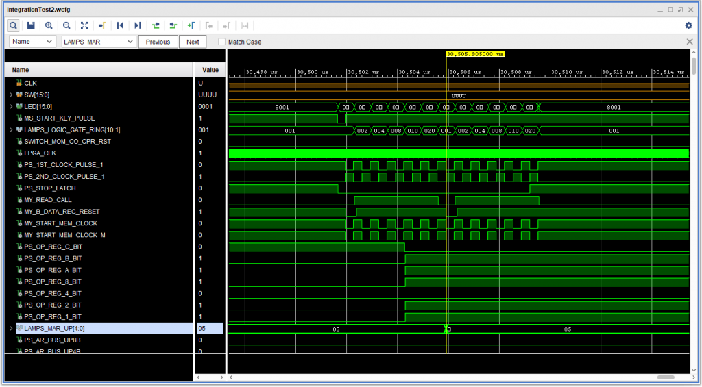
Here is the resulting timing diagram during simlation. The test code does a Computer Reset at the beginning of each iteration of the test 0 the first 3 do not set the conditions to start a read cycle, but the fourth one does. This matches up reasonably well with the timing diagram shown on figure 48 in the ILDs. (Not shown is the suppressed read with the Ten Thousands position 8 bit set.)
Note the long long delays here – about 425 ns for the B register reset (and activating the Y Read line), another 280 ns before activating the X read line, and then 1100 ns before deactivating the X and Y read lines. At 10ns per cell, that means 42 + 28 + 110 shift register cells. The Sense timing will add another 310 to 580 + 425 ns, and the write cycle will add 150 ns + 280 ns + 1200 ns – the grand total being 474 cells. Hopefully, I will have room without having to fudge them to preserve “slices” (each slice contains 8 flip flops and there are over 15,000 slices available in the chip on my development board.)
Oh, and have I … never mind. 8)
Reset and what was that?
Page 39.10.13.1 is pretty simple: a negative going read condition signal goes through two delay lines of 310ns and 0ns (which for now I have modeled as 10ns) to the AC set input of a trigger.
But there is a quirk: The first delay line is non inverting fed by a negative going input that goes through two inverters to get there – so it starts out as a 1. But the delay line initializes itself to 0 – it takes 310 ns for it to reflect that original input. During that time the output goes through the second delay line and manages to fire the trigger and activate the sense strobe (say what?). In the real world that would just result in garbage input to the sense amps.
The fix, in the test, was to wait for that all to settle out before activating the computer reset signal, but it took 15 minutes to figure out what was going on. In the original machine there is a delay of 25 microseconds between power good and issuing the system wide reset, which would take care of this just fine in the real world.
One issue I have seen in all of the memory timings is that the setup time for the triggers is quite long, and so pulses end up being longer than they should be. The Sense pulse should be somewhere just about 500ns according to the waveform diagram on ILD figure 48 and the . Mine is 525 ns. I am going to have to watch the relationship between some of these and the logic gates to make sure they don’t last too long or start too late.
With this, the memory pages are done, leaving just the IBM 1415 Console – the “fun” there will be the Selectric I/O portions.
The “Ghosts” in the 1410 Mode Switch
The IBM 1410 Mode switch had 6 labeled positions: C.E. (at the bottom), I/E Cycle, Address Set, Run, Display and Alter. Naturally there were 6 detents on the rotary switch that accompanied those positions.
Now, when entering the 1410 bootstrap, the usual sequence was to set the mode switch to address set, press Start, enter 0000 with the Load switch to +1, turn the Mode switch to display, press Start, enter 00000, wait for a bunch of “bbbbbbbbbb” to type out, press margin release (which allowed one to then enter multiple word marks later), turn the Mode Switch to Alter, press Start, enter the tape boot sequence (A WordMark+L % B 0 0 0 0 1 2 $ WordMark+N), turn the Mode switch to Run, press Computer Reset and then Start.
Note that I never mentioned pressing the Stop button. Well today, in looking at the ALD, I noticed that the switch actually has twelve positions (one of which is not actually shown on the ALD as it should be on block 5E). Every other switch position generates signal “-Y CONSOLE MODE SW STOP POS”. So, whenever the Mode switch is turned between two positions that are labeled (and have detents) it passes through another un-detented “ghost” position which activates a Stop condition. Clever.
Fits with Switches
Switches have been kind of problematic all along. Most of them signal active low when they are ON – so much so that rotary switches take that as their default. But momentary, toggle and “ALT” (which act like toggle) switches are mixed bag.
On top of that, switches, especially rotary switches, have multiple decks, and it is important to keep the switch positions aligned, bit wise, to make life easier later. So it took a bit to track down the switch decks on other pages and make sure they were in sync. Fortunately, only one of them was not: the Check Control switch deck on page 13.42.10.1 .
This sheet has toggles set up three different ways: The “Write Inhibit” toggle (which is actually unlabeled) creates an active LOW signal (logic 0, negative voltage) when OFF. It is the only switch in the bunch which works with the default settings. The “Auto Start” toggle creates an active LOW signal from the N pin when ON – in other words, active low. The “Inhibit PO” (print out) and “Asterisk Insert” switches create active LOW signals from their T output when OFF – also a sign of active low. It took me more than an hour to get my head around all of the toggle switches.
Page 40.10.03.1 as a bunch of switches. Most of the rotary switch decks and even the toggle switches (except 1 of each switch type) on this page have the grand task of turning on the “OFF NORMAL” lamp when any switch is not in what IBM was deemed the normal operating position. Two of the rotary switch decks (address entry deck 2 and storage scan deck 3) connect up in a kind of “and” gate via an isolating diode.
The Off Normal Lamp is also tricky: it lights when it’s input is logic 0 – being driven directly by the switches which are connected together. This ended up being the first “DOT” function that needed to be something other than AND or OR (besides the fact that it is fed from a mixed bag, so the HDL generation code punts that to an OR). What it in fact needs to be is a NAND: any logic 0 input (negative voltage) lights the lamp.
All told it took me more than four hours to get code generation patched up to segregate switch decks based on the info in their logic blocks (which IBM puts in the input and output level fields (which normally contain things like “S”, “B”, and “Y”)), fix other pages, write the test code and get my understanding of the switches operations to get it all working right.
I’d bet they will give me fits when I try and integrate multiple toggle switch decks together, too.
Fun with Latches
Most of the latches in the IBM 1410 are pretty straight-forward: the left side is usually the “Reset” side – a zero on an input to that side usually resets the latch, and the right side is usually the “Set” side – a zero on an input on that side usually sets the latch. Of course, one ought to avoid having 0 inputs on both sides, which would result in undefined behavior.
But sometimes latches can be reset another way: by having all ONE inputs on the SET side – which results in a zero on the reset side. Such is the case with the Console Stop Cond Latch on page 44.10.01.1. There is a “DOT” connection on one input of the “set” side – which happens to also be the output of the reset side. Two signals can reset the latch: Program Reset or the Inhibit Print Out switch. Easy enough. But testing this page got tricky because that DOT-ed connection is also an output (+S CONS STOP PRINT COMP COND).
When I first started testing, I just made that the NOT’ed output of the latch – since it was the output of the reset side of the latch. HOWEVER, that particular signal is also asserted if either of the two reset lines mentioned above is asserted – regardless of the state of the latch. Took me waaaaaaay too long to figure that out until common sense kicked in: that signal should be asserted if either the latch is reset OR either of the reset lines is asserted, stopping the printout.
“There You Go Again”
The quip from Ronald Reagan seems to apply to triggers. In this case, card type TAM, on page 45.20.02.1 – the console Y matrix (state machine) for dealing with 5 character addresses. In this case, the card type has its own VHDL file to implement it, because it is a trigger. Generally, I derived those from the logic and timing diagrams in the System Fundamentals – which for TAM is figures 113 and 114 on page 95. But something seemed odd, looking at the following connections for Y2, using those figures as a guide
| Gate | Signal | AC Pulse | Signal |
| Gate ON 1 | Y1 | AC Set 1 | MX Y Drive |
| Gate ON 2 (Pin F -really E) | MX ADDR DRIVE | AC Set 2 (Pin E – really F) | Y1 |
| Gate OFF 1 | Alter . Y2 . MX X6 OR Y2 . MX X1A | AC Reset 1 | MX Addr Drive |
| Gate OFF 2 | Set Y3 (MX X6 . Y2) OR (Not Alter . Not Read . Not Write . MX x6 . Y2) | AC Reset 2 | MX Y Drive |
As I was trying to make my tests work, I actually constructed the table above. It seemed “off”. The AC inputs are capacitator coupled (and not just for speed up – there is no parallel resist0r). Checking the Y3 trigger showed the same pattern, so it wasn’t just that the ALD had them reversed. Then, reading through the description in the IBM 1415 console manual, S223-2648, there was no hint of this situation.
Finally, I looked at the circuit diagram. Sure enough, E is the GATE input and F is the AC Pulse input – the System Fundamentals manual had reversed them. A quick use of my application’s card report revealed that this page was also the first time I had seen Gate On 2 / AC Set 2 used.
Fortunately, trivial to fix: all I had to do was go into my application card pin editor and swap the HDL signal name mappings for pins E and F (ACSET2 and GATEON2).
Have I… (“well…. never mind” — Paul Simon).
The 1415 Console I/O Selectric
Triggers and Latches and Cams – Oh My! (And latches driving triggers, driving latches – yeesh). Lots going on here, that made for some slow testing.
I will have some choices to make as to where I decide to “pick off” console output characters – either at the BCD level or emulate the various cams and solenoids. Of course, eventually I’d like to do the latter – frankly, I am a bit surprised that nobody has done that before. The I/O Selectric interface for inputs from cams happens on various pages, but the output magnet selection can be found on ILD figure 85. But for expediency, during my early testing I may decide to do it at the console character level.
However, while entering page 45.50.06.1 I found an error in the ILD. The IBM 1415 console manual, S223-2648 and the ALD agree that magnet R2A is “picked” when the input bits include either the 8 bit or not the 4 bit. The ILD incorrectly shows it being not the 8 bit (incorrect) or not the 4 bit (but the little chart at the bottom right of figure 85 does show R2A correctly.)
More errors were found on the ILD while working on page 45.50.07.1. For solenoid T1, the logic diagram shows a term in the equation of not 4 bit. The ALD and the table show that as not the A bit. Similarly, the logic diagram shows not 8 bit as a term for solenoid T2, but the ALD and the table shows that as not B bit. Finally, the ILD and the table on the ILD show the C bit as a term in the equation for the CHK solenoid, however the ALD and the IBM 1415 Console manual show this is really not the C bit.
The rest of the pages for the IBM 1415 were uneventful.
IBM 1410 ALD to FPGA Volume VIII complete – only two to go
Volume VIII started off pretty uneventfully, for a while. I did find another page (16.20.02.1) where a couple of gates have their internal connections brought to the edge of the sheet, but those are trivial to fix by adding “faux pins” to the gate definitions and using those on the sheet.
I continue to be somewhat surprised that I haven’t found very many connector errors – a testament to the value of verifying gate and signal use counts on each sheet.
Also, the number of ILD diagrams I have checked off as being completely tested in the CPU section is approaching closure. Of 65 such ILD diagrams, I have completely checked off the diagrams in all but 15 of them. (In addition I have quite a number of additional diagrams of the ILD ilk (i.e., drawn as positive logic with AND and OR gates, etc.).
Page 16.20.10.1 was a bit more interesting. On the surface, it is just a couple of latches. However, the corresponding diagrams on ILD figure 31 were in error. The outputs of these latches go to DOT-ed connection. While they are not like triggers in that they don’t “pull over” the output directly, they DO form part of the feedback loop for the latch, and thus can cause it to set (provided nothing else is keeping it reset). However, the engineer drawing the ILD didn’t take that behavior into account (and it did seem rather odd, just looking at the ILD, to have both a latch and a combinatorial group feeding the same output. ;))
In addition, on that same page, the latch comprised of the gates at 4E and 3E are unusual – the reset portion (4E) is a NAND gate, but at I first I thought that the set portion (3E) was NOR gate thinking that the engineer doing the ILD diagram did not spot it, which caused them to depict it as part of an “OR” to set the latch, when in fact those two inputs are effectively ANDed together.
However, when I ran into the same situation on page 16.20.14.1, the second use of card type YLH in my travels, I got suspicious and took a closer look at the circuit, which has a 3 diode DDTL (0-6V) *AND* circuit feeding an inverter/converter to SDRTL (-12V – 0V) – in other words, a NAND gate. This was actually the third card type where I had made this error – it caused me to go through all the card types I had interpreted as NOR gates to confirm that there were not any more such gaffes.
Page 16.20.15.1 had something else interesting. This is the Complement Latch page. There is also a related signal, “+B COMP ADD A” derived from that latch anded with “ADDER A CH USE T + C” (OR’ed with a couple of other things). The latch is set, among other ways, by the OR of a couple of signals “START COMPL ADD 1” or “START COMPL ADD 2”. Interestingly, “+B COMP ADD A” will also generate its output via (“START COMPL ADD 1” or “START COMPL ADD 2”) and that same “ADDER A CH USE T + C”. Since the effect of the OR part of this would also be setting the latch, it is in a sense redundant. I suspect that this might be in place get the +B COMP ADD A signal up just a tad quicker than the latch sets, by OR’ing it with the pair of signals that are also going to eventually to set the latch.
A “D’Oh” Moment
I had noticed in my travels that a number of signals end in asterisk or have an asterisk near the end. I had seen quite a number of them, particularly as inputs to DOT’ed connections on their destination sheets. But it wasn’t until I got to page 16.50.04.1 where what was logically an identical signal appeared with both a name without an asterisk and one with an asterisk (-B MPLY.MQ.B.B0 and -B MPLY.MQ.B.B0*) that I finally recognized what that actually meant – that those signals are indeed open collector outputs intended to be DOT’ed on their destination sheets. D’Oh. Sheesh – it took me two YEARS to catch on.
(Addendum: There are exceptions – probably when things were changed. Example: Page 17.13.06.1 generates signal “-S SET DOLLAR SIGN * EDIT”. However, this is a driven signal, not open collector and in most places, the “* EDIT” does not appear on the input side – only on page 12.12.51.1 does that signal appear with an asterisk – and it is not dotted. My guess is that originally there was an open collector variant, but they later found they did not need it.)
Signal Names Can Be Misleading
There are a lot of straight-forward if complex combinatorial sheets in this parcel of ALDs, and sometimes there is no corresponding ILD. In such cases I have been using the signal name to drive my test bench, but sometimes those signal names can be misleading. Case in point, on page 16.50.04.1 there is a signal name “-B MPLY.MQ.B.1.B0.BW” which implies Multiply OP and MQ latch and B Cycle and 1st Scan and B Channel 0 and B Channel wordmark. However, when I ran my test, it failed, because, looking at the ALD, it also incorporates the True Latch (usually represented at a “T” in the signal name dot sequence – but missing from this particular signal name.) I suppose that they added this factor somewhere during the design and testing phase, but didn’t want to bother renaming the signal to “-B MPLY.MQ.B.T.1.B0.BW”.
When a Space is NOT a Blank and vice-versa
Came across something interesting on the Edit Translator pages (17.11.*.1). These pages refer to “Blank” and “Space” as different characters. Say whaaaat? Fortunately, the ILD Figure 41.1 contained a hint: “NOT SPACE (NOT &)”. There are four BCD characters that have no number bits (bits 8, 4, 2 and 1 are all 0). “Blank” (no bits), – (Just a B Bit), Cent sign – which is also called “alternate or substitute blank” (just an A bit) and & – also known as “+” and, apparently, as “Space” (just the BA bits). I had been aware of the blank / alternate blank thing, because it appears in the principles of operation, but calling BA—- as anything but ampersand or “+” was a new one on me.
Keep on Learning, Learning, Learning
One of the fascinating things that has been going on throughout this entire project is learning to write test benches. Once I am through it all, I plan to post the generated VHDL on github, and this evolution will be very apparent. Ordinary VHDL of course, with signals, requires a flip flop/register/latch to remember state – they correspond to actual hardware logic signals. The IBM 1410 has a bunch of those latches, and some of them have “control” latches that remember something until the next major cycle comes around. What is more, often those control latches are hidden, i.e., their signals are not brought out on the ALD sheet. This presents a challenge in writing a test bench – because you need to know the state of that control latch from a previous iteration of the test vector to know whether the actual latch whose signal does appear as an ALD output ought to be. Even worse, some of these latches are in a latch loop – using the “visible” latch to “regenerate” the setting into the control latch until some kind of condition is satisfied. Up until today, I had been “remembering” that with code – which made writing the test bench both more intricate and complicated, and less complete as well. Enter another “D’Oh” moment: test benches can and do make use of VHDL variables, which, unlike signals, “remember” – they are like variables in most any other programming language. So, one can remember the *expected* state of the control latch, and then see if that results in the corresponding state of the “visible” latch on the next iteration. Better still, another variable enables the test bench to “remember” the state of the visible latch as well. This makes testing significantly easier and more thorough. The test bench for page 17.12.01.1 shows this new technique in practice. With this technique the latch testing on this page worked perfectly the first time – and was verified with the waveform trace in the simulator. BIG time saver here. Wish I had thought of it sooner.
(With apologies to Dory and Ellen DeGeneres. 😉 ).
   -- The variable declarations, VHDL wrapper declarations, etc. etc. are not shown here...

   testName := "17.12.01.1        ";

   MS_LOGIC_GATE_B_1 <= '0';
   MS_LOGIC_GATE_D_1 <= '0';
   wait for 30 ns;
   MS_LOGIC_GATE_B_1 <= '0';
   MS_LOGIC_GATE_D_1 <= '0';
   wait for 30 ns;

   check1(PS_NOT_0_SUPPRESS,'0',testName,"+S ZS Reset");
   check1(MS_NOT_0_SUPPRESS,'1',testName,"-S ZS Reset");

   for tt in 0 to 2**10 loop
      tv := std_logic_vector(to_unsigned(tt,tv'Length));
      d := tv(0);
      e := tv(1);
      f := tv(2);
      g := tv(3);
      h := tv(4);
      j := tv(5);
      k := tv(6);
      l := tv(7);
      m := tv(8);
      n := tv(9);

      g1 := g and h and k;
      g2 := g1 or (k and l) or m or n;
      g3 := d and e;
      g4 := (lastNotZSLatch and g2 and e) or g3 or (e and f and k);
      -- Note that g4 (gate 4) depends on the state from the previous iteration!!

      lastNotZS <= lastNotZSLatch;
       -- These two signals are just here so that I can see the variables on the "scope" waveform trace
      lastNotZSCtrlA <= lastNotZSCtrl;   -- There declarations appear before this "code" nearer the top of the test bench and are not shown

      -- Reset Not 0 Suppress Latch

      MS_LOGIC_GATE_B_1 <= '0';
      wait for 30 ns;
      MS_LOGIC_GATE_B_1 <= '1';
      wait for 30 ns;

      check1(PS_NOT_0_SUPPRESS,'0',testName,"+S ZS Loop Reset");
      check1(MS_NOT_0_SUPPRESS,'1',testName,"-S ZS Loop Reset");

      -- If Not ZS Ctrl was set last iteration, then set Not ZS Latch now

      PS_LOGIC_GATE_C_1 <= '1';
      wait for 30 ns;
      PS_LOGIC_GATE_C_1 <= '0';
      wait for 30 ns;

      check1(PS_NOT_0_SUPPRESS,lastNotZSCtrl,testName,"+S ZS From Ctrl");
      check1(MS_NOT_0_SUPPRESS,not lastNotZSCtrl,testName,"-S ZS From Ctrl");

      -- Reset Not ZS Ctrl  This should not affect Not ZS Latch

      MS_LOGIC_GATE_D_1 <= '0';
      wait for 30 ns;
      MS_LOGIC_GATE_D_1 <= '1';
      wait for 30 ns;

      check1(PS_NOT_0_SUPPRESS,lastNotZSCtrl,testName,"+S ZS From Ctrl Reset ZS Ctrl");
      check1(MS_NOT_0_SUPPRESS,not lastNotZSCtrl,testName,"-S ZS From Ctrl Reset ZS Ctrl");

      -- Remember the setting of the Not ZS Latch for the next iteration

      lastNotZSLatch := PS_NOT_0_SUPPRESS;

      -- Now maybe set Not ZS Ctrl

      PS_LAST_INSN_RO_CYCLE <= d;
      PS_LAST_LOGIC_GATE_1 <= e;

      PS_SIG_DIGIT <= f;
      PS_1ST_SCAN <= g;
      PS_NOT_CTRL_0 <= h;
      PS_E_OP_DOT_B_CYCLE_1 <= j;
      PS_E_OR_Z_DOT_2ND_SCAN_DOT_EXTENSION <= k;
      PS_BLK_0_PUNCT_OR_SIG_DIGIT <= l;
      MS_A_CYCLE <= not m;
      MS_3RD_SCAN <= not n;

      wait for 30 ns; -- Perhaps set Not ZS Ctrl

      -- Remember the *expected* state of Not ZS Ctrl for the next iteration

      lastNotZSCtrl := g4;

      -- Reset the signals before the next iteration

      PS_LAST_INSN_RO_CYCLE <= '0';
      PS_LAST_LOGIC_GATE_1 <= '0';

      PS_SIG_DIGIT <= '0';
      PS_1ST_SCAN <= '0';
      PS_NOT_CTRL_0 <= '0';
      PS_E_OP_DOT_B_CYCLE_1 <= '0';
      PS_E_OR_Z_DOT_2ND_SCAN_DOT_EXTENSION <= '0';
      PS_BLK_0_PUNCT_OR_SIG_DIGIT <= '0';
      MS_A_CYCLE <= '1';
      MS_3RD_SCAN <= '1';

   end loop;
IBM 1410 ALD to FPGA: Volume VII Testing Now Complete
Volume VII started off interesting right off the bat with page 15.49.01.1. First of all, I ran into more cases where “B” level signals fed into DOT functions, and recognized these situations are ANDs because the gates transistors go to 0V when on (logic 0, rather than one) and go to 6V when off (logic 1, rather than 0). Any single transistor turning on is enough to bring the signal to logic 0 – a logical AND. This triggered a move to have logic generation recognize when a DOT function is feeds a gate with a “B” level input or feeds a sheet edge with a B level signal, and makes it an AND – which I then later changed to snagging the logic function to use out of the signal levels table.
Also, on this same page, I discovered that I had mis-interpreted the logic function for two logic gates on card type DND as NOR, when they are actually NAND. As a result of investigating what to do about page 15.50.05.1, I also discovered I had goofed on card type YLJ as well, confirmed by comparing the logic on page 16.20.13.1 with the ILD figure 30. (Later I also found the same miss-interpretation for card type YLH).
Trouble in River City, page 15.50.*.1
Page 15.50.05.1 (and, really, all of the pages 15.50.01.1 – 15.50.09.1) are problematic, because they are not for the IBM 1410 Accelerator feature. This feature uses a fair amount of DTL (IBM DDTL) logic to speed things up. The card location diagram for panel 11C3 shows the DTL cards, but the ALD’s I have don’t match, and generally use SDRTL. For the most part, it doesn’t matter to the actual logic that I will produce for the FPGA. Rather than figure out exactly what the DDTL would be, I have been deferring to the ALD’s. However, on page 15.50.05.1, I ran into a problem. that page takes two inputs not shown on the ALD to produce an output which is also not shown on the ALD (or ILD, for that matter) and that signal is used on page 15.50.10.1 – which is for the accelerator feature.
The input signals are: “-B B CH MIN+INV PLUS SIGN GATED” (which I will refer to as signal “A”) and “-B B CH PLU+IN MIN SIGN GATED” (which I will refer to as signal “B”). The page also produces an output signal, “+B B CH PL+INV MIN SIGN GATED”, which I will refer to as signal “C”). Note that the wording of the output signal is slightly different than the input signal “B”, and is also +B vs -B.
Page 15.50.10.1 also uses signal “A” “-B B CH MIN+INV PLUS SIGN GATED” which originates on page 16.16.06.1, and it is , logically speaking (B CH Minus and Use B Ch Sign) or (B Ch Plus and Use Inv B Ch Sign) as one of many signals that can set the NOT Zone C Bit.
The ILD for page 15.50.10.1 does not match the ALD – it shows a pair of signals used among others in a large “OR” arrangement to set the ASSM Ch Zone C Bit: B CH Plus Sign Gated and B CH Invert Minus Sign Gated – which clearly matches signal “C”), and does not show “A” at all.
The upshot is, the equation for signal “C” might be as simple as C <= not B, but it is quite possible that it should be C <= not B and A. That latter equation would be equivalent in most circumstances, should not be harmful, and would automatically prevent this signal from setting the Zone C bit when its partner (signal not A) is setting the NOT Zone C bit – so that is what I chose to do.
To make that happen, I “fudged” some gates. I had on sheet 15.50.05.1 a DND gate (B level inverter) and a YLJ (NAND, B level input S level output) from the card location chart (which is for the accelerator feature) that I was not actually using as they don’t appear on the ALD. That combination produces NOT(NOT “B” and “A”) – the desired logic, but at a “-S” level. But 15.50.10.1 expects a “+B” level input. So I “tacked” on a gate “borrowed” from card type YLK 11C3F05. YLK is a an inverter accepting “-S” level input and producing “+B” level output. I doubt that this is how it was actually done, but since my ALD is using mostly SDRTL (“S” level) logic, and there aren’t any accelerator feature ILD’s, I went with this approach. Time will tell if it works.
Back to the more mundane stuff
On page 15.62.01.1 I discovered a signal name error. Usually I catch these the first time I come across them. This one was a little different, because the origin page, being for the 1311 disk, is not present in my print set. On page 15.62.01.1 I had miss-read the signal as “-S RECEIVER LATCH*1311” when the correct signal name is “-S RECOVER LATCH*1311” – the latter also appeared on an earlier page as well. Easy fix.
Page 15.62.03.1, which controls the strobe of I/O data was a tiny adventure. First, although the VDHL I wrote to handle SMS gate type TAM has the capability of being forced reset by an attached DOT function, I hadn’t told the database to assign that function to the faux pin “T”. In addition, both of the triggers on this page have their gates tied to ground (since these are SDRTL, that means LOGIC ONE), but the database did not reflect that – an easy fix. Finally, the ILD figure 44 has an error where it shows the various buffer strobes going into an OR which feeds the forced reset on the E Ch Strobe trigger, when in fact they feed into the clock (gated set) input on the trigger. It was pretty obvious when the test I wrote based on the ILD failed the first time that forced reset came into effect.
Page 15.70.33.1, the last page in this volume, also had a signal name error: there was an extra blank on the signal name “-C CPU TO CH TAU C BIT” which prevented group generation from generating a bit vector for it. Easily fixed. (FYI, TAU on the IBM 1410 stands for Tape Adapter Unit).
Triggers are a Pain
In working on page 15.62.04.1 I was reminded that the SMS trigger circuits are a pain. I had already dealt with the fact that another single gate “DOT-ed” with an on or off output can force that output on (either the “on” output or the “off” output can be so affected.) A second issue, though, is that some inputs are typically AC coupled – edge triggered, if you will. That means tracking state, because once an AC coupled input has reached logic 1, it cannot trigger again until it goes back to logic 0. I had dealt with the edge triggering before, but on this page my test tripped up because the variables that were tracking the edge were undefined. That bit me for the first time on this page, because I had neglected to force the trigger counters (4 of them, as there are 4 AC inputs, each requiring tracking 3 FPGA clock pulses to look for a logic-one-going pulse) to reset when the trigger is forced to a 1 or 0 – just initializing them to logic 0 didn’t help. This issue cropped up with card type TAM, which I fixed, but could also happen with card type DEY or DEZ (and maybe others I haven’t run into yet) as well. Did I mention that triggers are a pain? 😉
And, indeed, page 15.62.05.1 had the same issue, with card type SMS_DEY. Did I mention that triggers are a pain? 😉
Another thing about triggers: sometimes they are daisy-chained together, which means one has to be very careful about the relationship between test assertions and clock pulses. In a couple of tests I had to save what the state of the first trigger in a chain WAS before clocking in the 2nd trigger, which sets the 2nd trigger based on the state of the first one, but also clears the first one. Did I mention that triggers are a pain? 😉
Work to do merging switches
Not surprisingly, several switches on the IBM 1410 are multi-deck affairs. Right now the HDL group generation code does not recognize them, such that if a group contains multiple decks of the same switch, it gets it wrong. What it ought to do is recognize when the name of the switch and its number of positions match, and use a common bit vector for them. Until this gets fixed, I have to either test such pages separately, or tweak the generated group and test bench by hand.
1410 ALD to FPGA Volume VI is in the bag
The first adventure in Volume VI was on page 14.50.08.1, which generates +S INDEX REQUIRED and +S INDEX NOT REQUIRED . (They are not simply inverses of each other). The ILD figure 21 depicts part of the index not required signal as 1401 mode and Index C tag and NOT Hundreds position B and NOT Hundreds position B. When I wrote the test bench based on this it failed. No wonder: the 1401 uses the TENS position for indexing. The ALD itself was correct – the ILD was wrong. I actually don’t mind these kinds of “adventures” as long as there are not too many, as it validates the process I am using for testing when I catch errors like this.
Immediately following that was another non-adventure. The ILDs list ALD pages in ALD page order near the end of the ILDs. That table references 3 pages, 14.61.02.1 (twice, which is odd in and of itself), 14.61.03.1 and 14.61.04.1. However these pages are not listed anywhere, and no signals flow to or from them – they are completely nonexistent. These entries reference figure 24, which in fact covers pages 14.16.*.1. So, the table is simply wrong.
I am now using the new technique where I generate a test vector from an integer counter to test pages that don’t have latches or triggers. This creates a more thorough test, and as I get more comfortable with the process, it is usually quicker than what I had been doing.
A very curious thing happened on page 14.71.32.1 using this technique. There was a time period when the main output signal, to read out the C address register on the waveform trace was, well, blank – it was not ANY valid STD_LOGIC value. Yet VHDL code that was added to check to make sure the value was either ‘0’ or ‘1’ did not detect anything amiss. Finally, in desperation, I added a slight time delay before setting the variables that were changing the most slowly on the test vector which affected the output, and the anomaly went away. The equations that were generated from the ALD look fine, so I suspect it was some kind of bug in the waveform display code in Vivado 2018.2
Page 14.71.41.1 proved challenging. First, I found I really have not implemented switches right, so for now I am faking it a bit in the test benches. Secondly, there was a discrepancy between the ILD and the ALD for signal “+S ADDR MOD SET TO ZERO”. The ILD shows a term for an and which is NOT 1401 STORE AR OP CODE *AND* NOT 1ST SCAN CTRL. However, the ALD actually implements NOT 1401 STORE AR OPCOD *OR* NOT 1ST SCAN CTRL. Have to ponder which is right, but usually the ALD is. This is not the first discrepancy – I should have been better at documenting them as I go.
Page 14.71.51.1 had a different challenge: it has 2 input signals and one output signal that are referred to from other pages, but don’t actually appear on the sheet. Signal +S LOGIC GATE E2 is an input and +S STOP AGE G*ARITH is the other “extra” input (the latter from page 16.42.04.1). The output signal is clearly a NAND of these two: -S STOP AT G . LOGIG GATE E used on page 12.12.31.1, as are most of the other signals originating on this page. The only question is that the rest of these sorts of signals also feed a DOT connection to generate -Y WRITE CALL. My guess is that this one would as well – but I did not research it. As for gates, fortunately the card type TAU at 11C1F12 has an available gate (#2) that fits right in with the rest (and is also used on this page).
Another missing page has also been recovered: Page 15.41.06.1, which detected a record mark on the A Channel (The A and B “channels” are not I/O Channels, but rather really just busses inside the machine). In this case it was easy: the card location chart showed 8 gates of type DFF, which is almost identical to page 15.41.03.1.
A really interesting thing happened on pages 15.41.04.1 and 15.41.07.1, which detect blanks and group mark characters with word marks on the B Channel. These pages use DTL logic, with +B logic levels. However, though the system fundamentals manual which depicts DTL as using voltage levels of +Y 0V for logic 1 and -Y or -6V for logic 0, these sheets are using +B as +6V for logic 1 and -B as 0V for logic 0, and instead the gates using pull “ups” to logic 0 (a negative voltage), they have pull ups to +6V – logic one, and if the output transistor turns on it pulls the output DOWN to 0v – like traditional DTL — and the system fundamentals manual doesn’t describe that (it was added for the Accelerator feature which reduces the machine cycle time from 4.5us to 4.0us). Furthermore, on both of these sheets, the outputs from more than one gate are “DOT” ed together. With +S/-S or +Y/-Y logic, when gate outputs are joined, if one transistor turns on it brings the output to 0V – the DOT function therefore acts as an “OR”. However, with +B/-B, the transistor still brings the output to ground – but for +B/-B ground is logic *zero*, thus the DOT function behaves as an AND.
I had anticipated that I might run into this – in away I am surprised it took so long. So, I modified my application so that I could explicitly specify the logic function for a DOTed connection. (If this were in wide use, I’d also modify it so one could specify the default on a per-machine basis.) This change will also be helpful when I eventually go back and fix how switches work. Another great thing about this issue was that I caught it running my tests. It is good to have tests fail when they ought to. 😉
This also cropped up on the first page of Volume VII. It would probably be possible to automate the detection, based on the output logic level of the gates feeding the DOT Function being “B” or, alternatively, for the destination for the DOT function being a gate or sheet edge signal with logic level B. But, for now, I am holding off on that until I can write a report that looks at the DOT functions to make sure changing it now would not break anything I have already generated. I am thinking of adding a column to the logic levels table to set the default for based on logic level.
Page 15.41.12.1, which generates the E Channel Reset also presented a challenge. Pages that feed it send it signals for I Ring 2 time and for E CH Wrong Length Record (the latter being page 13.63.03.1), however page 15.41.12.1 does not use either signal. I caught this one with the test, as well – I had entered the sheet using the aforementioned wrong length record signal. Upon examination, page 15.41.12.1 is a later ECO that 13.63.03.1, so I changed it to match the ALD, using I Ring 1 Time instead of the wrong length record signal.
One other milestone that I crossed while working on this volume was that the first of two pages of the ALD sheet to ILD index was finished.
These all point to being well over half-way done with this process!
IBM 1410 ALD to FPGA: Volume V complete – a “quickie”
No, not that kind of “quickie”. Instead, it is about Volume V of the ALDs – now tested – in just over a week! This was due to a couple of related factors. The first 30 pages were address registers – continuation from the end of Volume IV. Then after a few more pages, the memory address register pages were up.
The second factor was a new testing technique. For cases where there are and or and/or or or gates that are similar (fed from a character of storage or another register), I started using a test vector generated from an integer counter, and then checked the results using straight-forward logic equations derived from the Instruction Logic Diagrams (ILDs), which allows me to zoom through those kinds of pages.
I also evolved how I test control signals. I typically don’t test those exhaustively with a loop (especially when they feed a latch or trigger), but I started a copy-paste routine with the variables that lets me build the tests a bit more quickly.
I really wish VHDL had a macro facility or call by name (or reference) capability, though, so I could write procedures that modify signals in a test bench. It would allow me to write generic and, and/or and or tests for various numbers of variables. Sure, I could generate the HDL with an external program, but that would actually take more time than the copy/paste technique I am currently using.
Volume V is the first volume that uses NOR (primitive DTL) for actual logic. NOR logic also shows up in gated input interface signals, but that is a different animal. I was only about 90% confident of my interpretation of some of those circuits, but so far they have been spot on.
Volume V did present a few challanges. First, another missing page: page 14.18.04.1, part of the zone adder, was missing in action. It was clearly a copy/assembly error when the drawings were assembled – page 14.18.05.1 appears twice on both sides of the same sheet: one of those shoud be 14.18.04.1.
Now, I could easily have just replicated the ILD as equations, but I took it a bit further than that, consistent with what I have done on other missing ALD pages. Research based on the card location chart uncovered that I had one card at 11C3A16 (type DEV) entirely dedicated to this page, though the chart only showed four of the seven gates on that card actually being used. I also discovered that the card at 11C3A17 (type DFS) had 3 gates dedicated to the cause and by elimination of a gate or two that appeared on other sheets I was able to determine which gates/pins were “available”. I struggled for a day to make it work with just 6 gates (3 from the DEV and 3 from the DFS) but I couldn’t find a way. So in the end I drafted the remaining 3 gates from DEV (which are a AND/OR triad) to complete the task. While this doesn’t agree 100% with the card location chart, who is to say that the card location chart wasn’t quite right. 😉
I did find a couple of ILD errors in this volume. On page 17 of the ILD, relating to ALD page 14.30.06.1 a couple of signals are inverted and depicted as feeding OR logic. In reality, these signals are inverted on the inputs (-Y – negative active) and ANDed together. It happened because that ALD happens to depict a single NOR gate as two – one feeding the other – because that card has more inputs than can fit on a single logic block in an ALD. The symbols on the gates on the ALD do indeed imply that all the inputs are ANDed together, but if one didn’t spot that both blocks involved are the same card gate, one could easily misinterpret it. Curiously, the same thing happens on page 14.30.05.1 (the previous page), but in that case the engineer who prepared the ILD interpreted it correctly.
Those same blocks on those same two gates allowed me to leverage a feature on my application. When I entered those logic blocks, I realized that they were, in both cases, the same gates. However, since they are next to each other on the ALD they were not candidates for using the “extension” capability to combine them – there would have been room for that on the page, but they were not depicted as extensions. So I moved the inputs from one of the gates of the pair to the other, and removed the output from that first one as well. When I first tried generate the HDL, the application noticed the unconnected gate and generated a (harmless) error. However, a while back I added the ability to tell the application to ignore a given logic block when generating HDL. Worked like a charm.
Another case where I ran into that sort of thing was on the real time clock, where a given switch “deck” was split in two, and also the block title — which I used to generate the name of a switch signal — was replicated between decks. In order to generate this correctly I had to tweak the logic block titles to separate them, and join the switches together in the test bench.
The ILD’s also, generally, did not include the gates for address wraparound from x9999 to 00000 for 60K and 80K – only for 20K and 40K machines. The wraparound logic was present on the ALDs however, and was easy to decipher. (Wraparound for 100K is automatic because there are only 5 digits of addressing. 10K machines to no support wraparound at all, if I recall correctly)
I discovered a typo on a signal name on page 14.17.10.1 “-S AR BUS GRD OUT THP0B” — GRD should be GTD (gated).
ILD figure 24 had an error relating to page 14.16.04.1 om calculating the Address Register Exit Channel “C” bit – at the least it didn’t match the ALD. In general I defer to the ALD after carefully checking the logic, figuring that the ALDs are later in the timeline than the ILDs.
I also found a case of a misleading signal name, where the signal name implies two factors in an AND, when there are actually three. However, going back I can’t seem to find it – I will update this page if I come across it.
Finally, I have come to dislike a certain idiom that has appeared on a handful of sheets, where a pair of latches are ins sequence, usually named “… Control” and “…” where the output of “…” resets “…Control”. A real pain to devise a test bench.