Overlapped Tape I/O is generally working OK now. Getting that to work involved two things.
Firstly, I needed a delay corresponding to the tape inter-record gap time (though not nearly that long) so that the several instructions that the diagnostic runs through before it tests for an overlapped condition would occur while an I/O Overlap still in progress. This fixed the error stop problem. Fortunately, that was much easier to find and fix than I had expected.
After fixing that problem, overlapped reads worked correctly, but overlapped writes had a problem – they somtimes dddduplicated characters 😉 – resulting in records longer than they should have been (and with incorrect contents).
The latter turned out to be more or less self inflicted. In August of 2023, I encountered some issues with the Store A Address Register (SAR) instruction. To fix that I used the +S ADDR MOD SET TO ZERO signal to inhibit resetting the modify by zero address modifier control latch, reasoning that latches don’t respond well to having simultaneous set and reset signals active at the same time.
In this case, however, that was causing the Modify by Zero Address Latch to not reset at times when it needed to, which then sometimes inhibited the Modify by +1 Address Latch from setting, causing the address for the I/O to not increment properly.
The fix was to modify the ALD that generates the address modificatio signals, ALD 14.71.41.1 ADDRESS MODIFIER CONTROLS to inhibit generation of the +S ADDR MOD SET TO ZERO signal in the presence of +S ADDR MOD SET TO PLUS ONE. For now, that was done directly in the VHDL. To fix it in the ALD I would need to add a couple of “phantom” gates.
The wrong length record issues when writing for locations ending at the end of memory remain, as does Error 17 involving the timing of longer inter-record gaps expected from a tape Erase call, and some other errors involving the 2nd channel (tape marks? backspaces?) still remain.
The vast majority of errors noted by the tape diagnostic T020C related to wrong length record errors, particularly when a tape operation writes from the last character of storage (39999 in my current 40K implementation), usually starting at location 39990.
The current FPGA from the ALDs implementation does not create an error stop, it simply writes until it has written the character at location 39998 and stops, with a wrong length record (WLR) error – with one less character written than the diagnostic would expect, as well. (Then, subsequently, the read operations in the tests also generate WLR because they are expecting 10 characters, but only get 9).
Part of the problem is that various documents describe what should happen in such a case differently:
Diagnostic T020C (1964):
The diagnostics do not expect an WLR when writing from the last location in core storage or reading into the last location in core storage. (A WLR would presumably occur when reading into the last location of core storage if the record extends beyond that character.)
A22-0526 (no suffix) 1963
Addressing: During execution of an instruction, no address must be decremented past 00000 or incremented past the highest valid address. This includes operations that act on data in a single position only; such operations will be executed but, after the operation the associated address register will contain an address beyond one of the limits and the system will stop and signal an error.
Tape: WLR is never set on a Write or Unit control operation, unless the record is of zero length, i.e. the character at the start is a Group Mark with a Word Mark.
Tape: Read to End of Core ($): Reads until the last storage position is filled.
Tape: Write to End of Core (X): Writes until the last storage position is encountered. [ed: to me this is a little vague: does it mean that the last character storage position is written from, or not?]
Console I/O: WLR is never set (I have not yet tested this)
A22-0526-3 (1961) and A22-0526-2
Addressing: If an operation increments addresses, 59998 is the highest position (assuming a 60K system) that can be referenced or in which data can be read or inserted as the result of an instruction. If 59999 is addressed in an incrementing operation, the system will stop and signal an address check. There are two exceptions: 1. A manual console operation; that is display and alter. 2. Data may be read from or inserted into 59999 without causing an address check in the execution of a read or write “to end of core” I/O instruction.
Tape: WLR (W-U) Never set (unless record is of zero length and first character written is GM/WM)
Tape: Read to End of Core ($) and Write to End of Core (X): read/written until the last core-storage position is encountered. (Notice that this older document does not specifically differentiate between the read and write behaviors)
The ALDs for my machine in these areas are all dated 1962.
Because this issue is unlikely to cause operational issues, I expect to “table” it for now and revisit it later. It may be that ECOs were required to change the behavior to what is expected in the diagnostic.
UPDATE: This turned out to be very easy to fix. At first I tried all sorts of things to try and control the setting of the Internal End of Transfer Latch by inhibiting setting that when the channel Wrap Condition was asserted — but that led to an address check as the 1411 CPU tried to fetch the next higher location, instead of wrapping around to location 0.
So then I decided that I would just make a change to the ALDs on pages 13.71.05.1 (E Channel) and 13.66.09.1 (F Channel) to suppress the MC_DISCONNECT_CALL to the TAU while the E2/F2 register was still full. That worked — even better than I expected. Not only did that cause it to write out the last location of memory, it also caused the Wrong Length Record status to go away as well.
That left me with ONLY ERROR 17 on the E channel. The F Channel had ERROR 17, but also errors 20, 23 and 70, which seemed odd. But otherwise, both channels read and write tape just fine.
Error 20 occurs when a tape mark is read, and the diagnostic expects that the CPU will also set the CONDITION status for the I/O operation, but it was not setting the CONDITION status.
Seeing that some of the problems that I had identified with the Tape Adapter Unit (TAU) implementation could be or might be traceable back to the fact that I was using a 115,200 bps serial over USB to communicate between the 1410 FPGA implementation and the PC side support program, I decided to look at alternatives.
I2C would be too slow, and I would need some kind of intermediary like a PIC or Raspberry PI to talk I2C and then something else, like TCP/IP or UDP to talk to the PC side.
SPI, at 10Mbps would probably be fast enough, but also would need an intermediary.
I could use an embedded soft processor, like a MicroBlaze, on the FPGA. That would probably work, but would take up a lot of resources on the FPGA, and I was concerned that the Xilinx XC7A100T might not have enough for all of the things I might want to do, especially with a TCP or UDP stack added in. I did do a little playing with Microblaze a few years back, and found the development process somewhat cumbersome: it would considerably lengthen all of the place and route everytime I made a change.
Understandably there do not seem to be any direct TCP implementations in VHDL or Verilog that I could find.
I found three different implementations of UDP, two in VHDL and one in Verilog that I decided to test.
Two of the UDP implementations were on opencores.org. They were old, apparently done as a research project, and it was not apparent how to configure it to work on my hardware, so I quickly abandoned those. Plus, it took opencores.org three months to grant my request for a user ID.
Next I looked at the UDP implementation from Alex Forencich. At the time, it was located at https://github.com/alexforencich/verilog-ethernet, however, that one has apparently been superceded by one at https://github.com/fpganinja/taxi — however this latter one seems to no longer include a UDP stack. This UDP implementation looked promising, however there were a couple of issues for me. Firstly, it used a generation process using cocotb. When I tried to do that, it did not work well for me. So, I ended up doing what it would have done to figure out what files I actually needed.
The second issue with this UDP implementation from Alex Forencich was that it was not directly complatible with the physical ethernet interface (PHY) on my Nexys4 development board. It is set up to interface with an MII layer, however, my Nexys4 PHY uses an RMII layer. I tried a couple of approaches to resolve this issue. The first was to see if the Ethernet MAC at https://github.com/chasep255/Nexys-4-DDR-Ethernet-Mac would work. It provides an AXI interface to the Ethernet MAC on the Nexys4 board, but also uses RMII. There was something important I cleaned from this latter project however: how to build a test bench to send and receive Ethernet packets, which I used quite a bit.
In the end I found a free MII to RMII v2.0 interface layer IP from Xilinx. While not available in the latest versions of Vivado, it was still there in my older versions of Vivado, and while not supported by Xilinx, it works fine in Vivado 2023.1, and I would expect it will continue to function OK in later releases as well. And, worst case I could also do a development board upgrade to something that has an Ethernet interface using MII.
It took me quite a bit of futzing around to get Alex Forencich’s UDP layer working as it was in Verilog, and I need to interface to it with VHDL. Also, the example/sample logic just does a UDP echo, and it took some time and testing to figure out how to separate out sending and receiving UDP packets.
Once I had it working, it was not tremendously difficult to integrate it into my 1410 FPGA logic. I chose to continue to use a stream UART-like interface that is as close as possible to what I had for an actual UART, so that only minimal changes were required in my existing state machines. I did need to expand the intermediary output related FIFOs from 8 bits to 9 in the logic, however, to carry a “flush flag” so that, for example, when the 1410 needed to send a UDP request for a tape operation, it could force the UDP layer to send the packet even though it was not full. Everything else remained essentially the same as when I was using a serial port.
I now use the UDP implementation for TAU related packets going both ways, to and from the FPGA, for lamp data going from the FPGA to the PC and for sending memory images (“core loads”) from the PC to the FPGA. I did find that I have to throttle the lamps some and not update them as fast as I’d like – the speed of the C# code and Windows updates are a limiting factor. I even found that on tape writes I had to add what kind of corresponds to a tape stop in the inter-record gap, to add a delay when writing so that it does not overwhelm the PC (which leads to lost packet(s) and a program error). I also added some delay when the PC is sending data back to the FPGA for tape reads so that it does not overwhelm the FPGA UDP stack.
With those changes, it can now reliable write and read tape records, though some tape related problems when running diagnostic T020 remain unchanged:
Error 17, caused by a test of the ability to do an erase operation to write a long interrecord gap over a bad stretch of tape.
Errors 39, 41 and tape I/O operations resulting in Wrong Length Record Status. The problem relates to what happens when writing a record that goes to the end of core storage (with no Group Mark + Word Mark) and reading records that go to the end of core storage.
In one of the later tests a read tape to end of core is executed, in odd parity. The tape data is in odd parity as well. However, the operation generates a data check, and core storage from 39990 to 39998 (for a 9 character record) are all asterisks from what the 1410 sees as an invalid parity.
On Channel 2 / F Channel, errors 20, 23 and 70 which seem to relate to problems when a tape mark is encountered after writing one and backspacing over it.
T020 starts by trying an overlapped write on each tape drive. If it finds one that is ready, the result is a 1410 error stop, I think on an “R” I/O status branch instruction, with only 1 byte transferred to the PC.
In May of 2024, I turned my attention to Tape I/O. On a real IBM 1410, this I/O would be routed through an IBM 1414 I/O Synchronizer (Model 1, 2 or 7, also known as Tape Adapter Units (TAUs). However, there were two issues with that for me. Firstly, I do not have ALDs for the TAU. Secondly, because the TAU expects to interface with a real tape drive, and I don’t have any, the timing would not work. Fortunately I soon discovered that the IBM 1410 channels don’t actually care about the timing – they are driven by the MC_TAPE_READ_STROBE and MC_TAPE_WRITE_STROBE signals from the TAU.
It took me from mid May 2024 to mid July 2024 to design the logic, test, and work out bugs to the point where I could load diagnostics from the diagnostic tape and they would run. This was a significant milesone!
Testing revealed several problems when running the first tape diagnostic, TU20:
Error 17. This error happens because my setup ignores erase requests which write long inter record gaps (IRGs), and the diagnostic expects to see different times (measured in a timing loop) when reading a record with a normal IRG vs. one after an erase with a long IRG. This is not a “real problem”.
Many errors displayed for reads and writes which involve the end of memory. The writes write records only through location 39998 before an internal and of transfer stops the transfer, and then the reads aren’t as long as expected, either.
Errors 39 and 41, which involve writes which try to read one character past the end of memory.
Problems with data transfer between the FPGA and the CPU using the serial port. There seemed to be data being lost during the lasts tests where 1000 records are written and read back twice causing the diagnostic to fail. This created a “crisis of confidence” of sorts – I need reads and writes to be reliable.
Data transfer between the FPGA and the CPU was much much slower than on a real machine – intolerably so – essentially a “non starter” with respect to much further progress.
The copy of T020 that is on the tape is set up to assume that the machine has overlapped I/O. Unfortunately, because of a bug in the FPGA of an unknown origin, the 1410 hits an error stop. This requires resetting the machine, changing the “TAD” at location 1004 to a 1 to suppress testing the 2nd channel, and then restarting at location 2000.
Not having confidence in reading and writing, and with the slowness of PC <-> FPGA transfers was a big concern. So, in August 2024 I began researching to see how I might use Ethernet instead of the 115,200 bps serial over USB that I had been using. That is the subject of the next post!
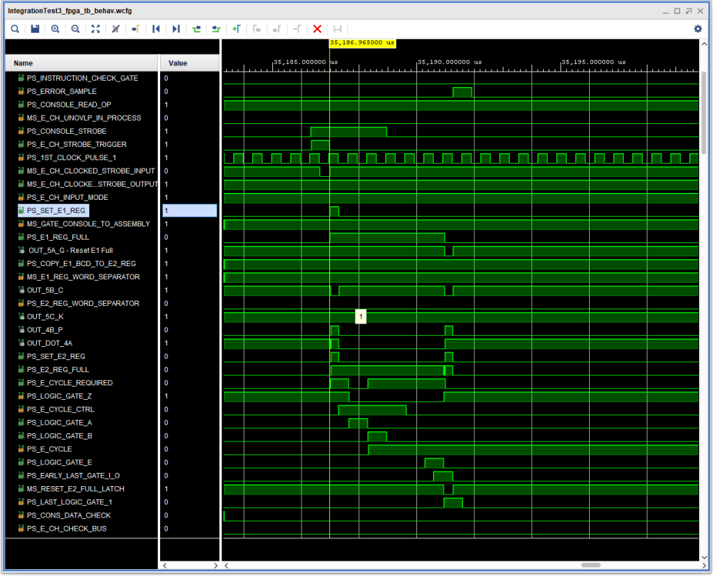
The next issue to fix was another instruction check, this one after a console input instruction finished where the number of input characters was less than or equal to the number of expected input characters.
The basic problem was that as I/O was ending, the I CYCLE CTRL signal goes active while E CH UNOVERLAP IN PROCESS is also active.
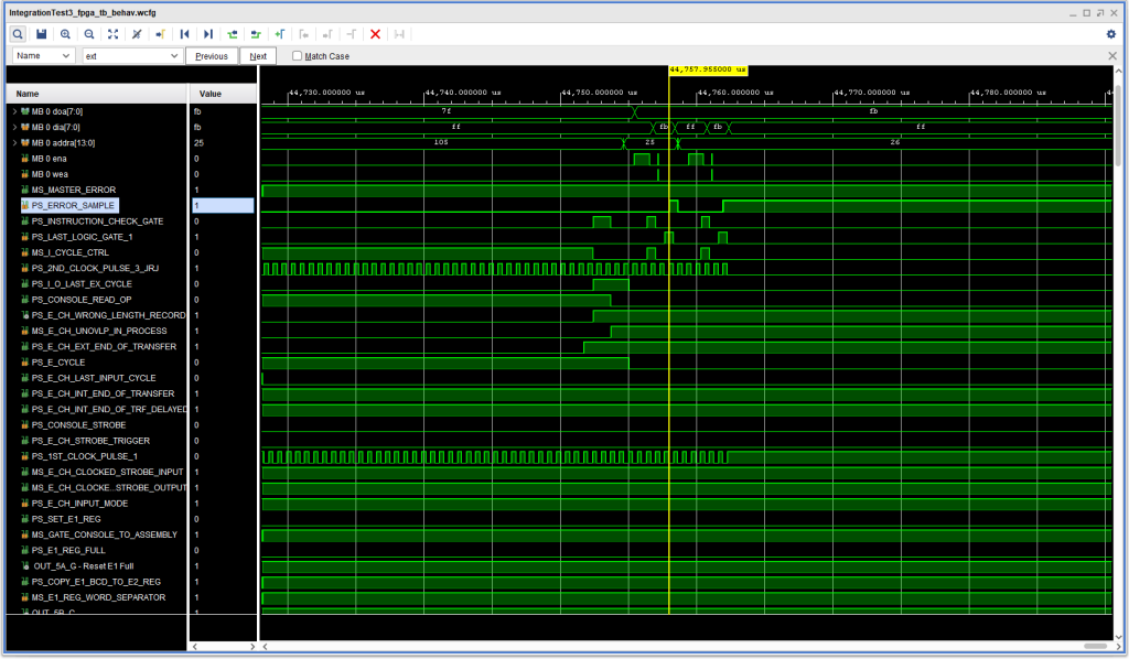
The problem can be seen in this waveform capture:
Instruction Check during completion of console input where the number of characters entered is less than or equal to the number of expected characters.
What made this problem a bit more interesting was that this error did not occur if the number of characters entered was more than the available buffer (i.e., from the address specified in the read instruction up to and not including the group mark with a word mark that marks the end of the input buffer:
NO Instruction Check during completion of console input where the number of characters entered is greater than the number of expected characters.
I spent quite a few days looking at this and that and trying this and that, without making much headway. And in the process I discovered a couple of interesting errors in the IBM CE documentation for the 1410.
One thing I noticed was that the logic for an Instruction Check that is shown in the IBM 1410 System Fundamentals manual, S223-2589 and is quite simple would not have caused this Instruction Check, and that the logic in the Instruction Logic Diagrams, R23-2936 does have logic that would trigger an error under these circumstances and is more complex. The latter matches (more or less — more on that later) the ALD and triggers this error from either of the bottom two sets of (ILD) AND/OR gates in the lower left hand corner of Figure 58 of the ILD. (In reality, these are implemented using AND/NOR gates – aka And/Or/Invert gates).
The second thing I noticed was that in the I-O sequence diagram on page 43 of the 1411 I/O Operations Manual 223-2692 depicts +S I CYCLE CTRL indeed overlapping +S E CH UNOVERLAP IN PROCESS – in contradiction to what is on the ILDs.
Finally, in comparing the ILD to the ALD I did spot one error in the ILD. In the bottom most And/Or gate on the ILD, there is an OR gate for signals E CH OVERLAP IN PROCESS and I CYC CTRL. In fact, that one is F CH on the ALD (which make more sense).
So, what to do. I had some concern that the change I made earlier to ALD page 12.12.62.1 to inhibit E Cycle Required during Logic Gate A might be a problem, but thought experiments didn’t bear that out. Also, the condition seemed to be benign, in that once the I/O completed, E CH UNOVERLAP IN PROCESS would be de-asserted. Finally, I wondered it this might be another case where the speed of the FPGA logic for multiple layers via LUTs – look up tables – might be causing a race condition.
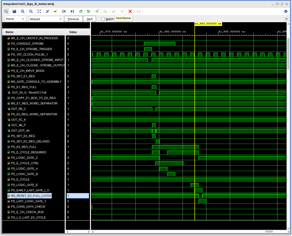
In the end, I decided on a simple approach. I created a variant of card type DHL, called DHLJ, with an extra direct input to the NOR gate, using otherwise unused pin K. I then fed in the I-O LAST EXEC CYC signal into ALD logic blocks 4E and 4H, which resolved the Instruction Check.
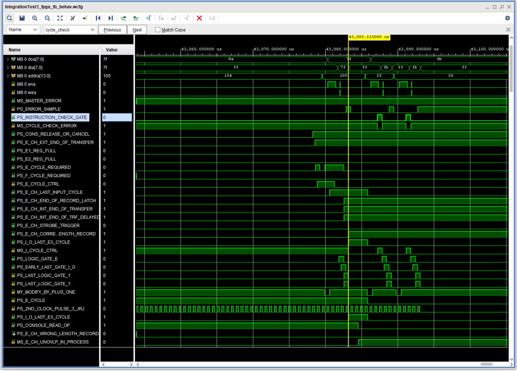
This is shown in the following timing diagram:
Input Instruction Check fixed by inhibiting an instruction check when IO is finishing up and +S I-O LAST EX CYCLE is active.
This isn’t the most satisfactory thing in the world, but given the contradictory nature of the IBM materials, I didn’t feel like I’d be able to sort it out properly – at least for now. (Also note in the above timing diagram the “notch” in +S E CYCLE REQUIRED during Logic Gate A, caused by the earlier fix.)
With this fix, there are no more problems running the 1410 diagnostic CU01C, nor the 1401 Mode diagnostic M011, including console input.
There is still much to do, including replicating the E Channel fix to ALD 15.41.10.1 into the F channel. After that, I think I will spend some time cleaning up console operations, where there are lots of things to change on the PC Support program software side, as well as some hardware issues, like the improper prompt character during the start of a console Display operation (and other operations as well), and some possible issues during address set and storage load and regen operations.
As mentioned in the previous post, during testing of the 1401 compatibility of the IBM 1410 I discovered that console input was not working properly for the machine in either 1410 or 1401 mode. The 1411 CPU would accept the characters, but only the first was entered into storage (if that), and pressing Inquiry Release or Inquiry Cancel did not terminate the I/O operation. After some trial and error signal examination, I discovered that the E1 Register Full latch was “oscillating”, and the cause seemed to be a simultaneous set and reset signals.
In the original hardware, this was unlikely to occur, given multiple layers of logic gates, signal travel times on the backplane wiring, and so on. But in a simulation, or in an FPGA the combinatorial logic signals are implemented using look up tables (LUTs) making instantaneously simultaneous combinatorial signals a likely possibility.
Timing Diagram showing problem with E1 Reg Full being set and reset at the same time.
So, how to prevent that? The first, more or less obvious thing, was to condition one or both of the set and reset signals to give one or the other priority. I found that if I gave the reset signal priority (by inhibiting set when reset was active) that console output was negatively affected, because this change affected both input and output.
However, if I added an inhibit from the set signal to the logic block at 5A, so that set for just input had priority, the problem went away – I could type characters into the console and they were properly entered into memory.
But I also noticed that doing the fix that way I ended up with second pulse of +S SET E2 REG during the cycle. While this didn’t seem to cause any real problems, I was nervous about possible future effects. In addition, it left the E1 FULL signal active for longer than it needed to be.
First attempt to fix E1 Set/Reset Latch problem resulting in duplication of +S SET E2 REG
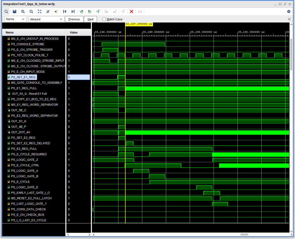
While looking at ALD page 15.62.04.1, which generates signal +S SET E2 REG, I noticed another signal, delayed by 1 IBM 1410 clock pulse, +S SET E2 REG DELAYED. Feeding that into the logic block 5A on ALD page 15.41.10.1 instead of +S SET E2 REG allowed an earlier reset of the E1 REG FULL latch to the time where it really should be happening, and prevented the extra +S SET E2 REG pulse from occurring.
Fix for E1 REG FULL latch problem by using +S SET E2 REG DELAYED
I am a little concerned about the +S E CYCLE REQUIRED being inactive during Logic Gate A, but it doesn’t seem to be causing any problems so far.
However, there is still one remaining issue with console input. If I enter more characters than are allocated in the buffer (terminated by a Group Mark with a Word Mark), the M%T0xxxxxR instruction ends normally. But if I enter fewer characters or the exact number of characters expected, the instruction ends with an Instruction Check, I think because I CYCLE CTRL and E CH UNOVERLAP IN PROCESS are both active at the same time. In the CE instructional text manuals, this check is not present in the logic, however in the ILDs it is present. The question is whether the test should not be implemented the way it is (perhaps by adding some signal to the logic), or if it is just an inopportune appearance of a Error Sample pulse at that time.
The last issue that I had running the 1401 diagnostic (aside from Console I/O input working in neither 1410 nor 1401 mode) was “ERR ?3S” in diagnostic M011A, which corresponds to diagnostic location 07032 (the routine actually starts at location 06980). This is test RN111, the very last test in the diagnostic.
The diagnostic comment block says it all:
RN111 TURN ON OVFVLW IND WITH ADD INSTR EXECUTE BR INSTR WITH UNITS PSN OF A ADDR CONTAINING Z TEST FOR OVLW IND STILL ON
Trouble was, the overflow indicator was indeed off after executing the branch instruction at location 7016 (which branches to location 7899, which was set up to just branch right back to location 7020.) What is so special about the “Z”? Well, it turns out the “Z” is the d-character for a B(I)Z instruction – branch on overflow (a sample of which is at location 7027). But why should that ever be in the Op Modifier register for an unconditional branch instruction that has no “d” character?
Well, it turns out that the 1401 mode instruction readout often places a character from the address into the Op Modifier register, as noted in the IBM 1401-1410 Compatibility CE Instructional Manual, Figure 3B on page 9.
There were a few possibilities for this problem, and a few possible cures for this. In the end, some simulation runs demonstrated that the reset occurred because “Z” was indeed still in the Op Modifier register when the unconditional branch was set up.
Simulation trace showing the Overflow indicator being reset during readout of a Branch Unconditional instruction with “Z” as the last character of the address.
There were several possible cures that might have fixed this, focused on the fact that in a normal B(I)d conditional branch the d character is read out later in the I cycle – so maybe one could reset the Op Modifier register after the address was read out and the following character had a word mark – indicating that the branch had not “d” character at all. But in thinking about it I wondered why this very specific test was in the diagnostic – and as the last test, which maybe meant this was an issue that was uncovered in the field (and perhaps only on machines with the Accelerator special feature).
The reset of the Op Modifier register is controlled on ALD 15.38.04.1. Interestingly, a very relevant signal, +S CHAR TEST BRANCH OP CODE that this page says originates on page 13.13.05.1, does not show up on page 15.38.04.1 as a destination. I had had to “add” that signal into the signal list when I came to page 15.38.04.1 when I entered the data for that page into the database. Perhaps more interestingly, the Instructional Logic Diagram for this ALD, part of ILD Figure 26, shows the signal as instead being +S 1401 COND TEST OP CODE , and is designed to reset the Op Modifier register when:
+S 1401 COND TEST OP CODE is active AND
In 1401 Mode AND
The B Channel has a WM Bit (i.e., end of the instruction) AND
Logic Gate D AND
I Ring 8 Time
Well gee whiz… this was exactly the kind of signal I was looking for to fix this problem. So, to fix it, all I did was change +S CHAR TEST BRANCH OP CODE on the ALD to the one the ILD specified, +S 1401 COND TEST OP CODE, and the problem was cured, with no side effects causing other problems.
Simulation trace showing the reset of the Op Modifier register during I8 time during readout of an unconditional branch instruction.
So this was presumably a case of either a) a mismatch between a page denoting it is for the ACC feature (15.38.04.1) and the source page of 13.13.05.1 which does not call out the ACC feature, or, perhaps, page 15.38.04.1 being “down level” – not having a necessary ECO t fix this. When I did the change, I set up an “ECO” JRJ005 in the database.
With this, the 1401 diagnostic M011A runs to completion without errors, as does the 1410 CPU diagnostic CU01.
During this testing, however, I discovered an issue affecting both 1410 and 1401 mode: Console I/O Input does not work – the characters don’t seem to make it into “core”, and when Inquiry Release is pressed, the I/O operation does not complete. This could be something as simple as a support console software bug or, more likely, an issue in the interface between the 1415 console emulation VHDL and the 1411 CPU Channel, since 1415 Console Input during console control operations (setting addresses, memory data, etc. all seem to work mostly OK). Time will tell.
So, not the yummy treats, but a new problem that showed up with the SAR instruction.
The fix to ERR 60J was pretty easy. That was a gate for feature S10 – a 10K 1410 that needed removing (and its output replaced by a logic ‘1’) on page 14.30.05.1. QED.
However, after fixing that, I then experienced an error near another Store A Address (SAR) instruction, at (just before) location 8624, exhibiting A Channel, Assembly Channel and Address Exit validity checks, with garbage in the B Address Register. However, when I ran the same instructions in the same place in the address space (but with memory otherwise all blanks) it seemed to work just fine. How could this be?
The first blind alley was either that the print chain used for the diagnostic listing printed the 1410 characters “?” and “!” as “&” and “-” respectively, or there was a bug in the listing version that was fixed on tape. So much for that hypothesis.
To figure this out it would be best if I could get it to fail under simulation (There is a scoping capability in the FPGA as well – but not as quick and easy to use.) As mentioned above, during initial testing for this problem, I just loaded the relevant instructions into the appropriate memory locations with memory from 10K up to 40K being blank characters and the failure did not occur. Further more, during testing I discovered that if I had only loaded the first 10K of the 1410 1401 mode diagnostic, M011, as the listing only went up to just under 9K, this problem also did not occur, and the only error ?3S (translated into address 07032). However, that diagnostic is ordinarily loaded from the 1410 diagnostic program TC50, and when I used the image that I have that goes up to 40K, all heck broke loose with the error noted above. I then changed my memory initialization to all ‘9’ characters aside from the instructions under test and was able to reproduce the issue under simulation.
This led me to an initial suspicion that something must be causing more than one B character register from “core” to read out simultaneously. Only one is supposed to read out at a time – and their outputs are OR’d together. If more than one read out at the same time, the results would be problematic. But how was this occuring?
After many simulation runs looking at various signals and what might be going on, I finally hit upon this one.
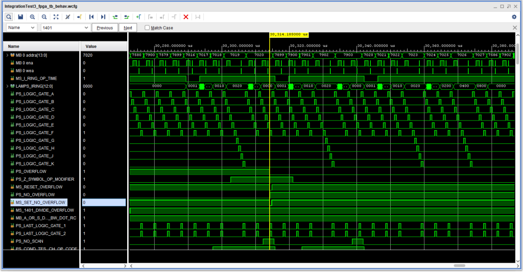
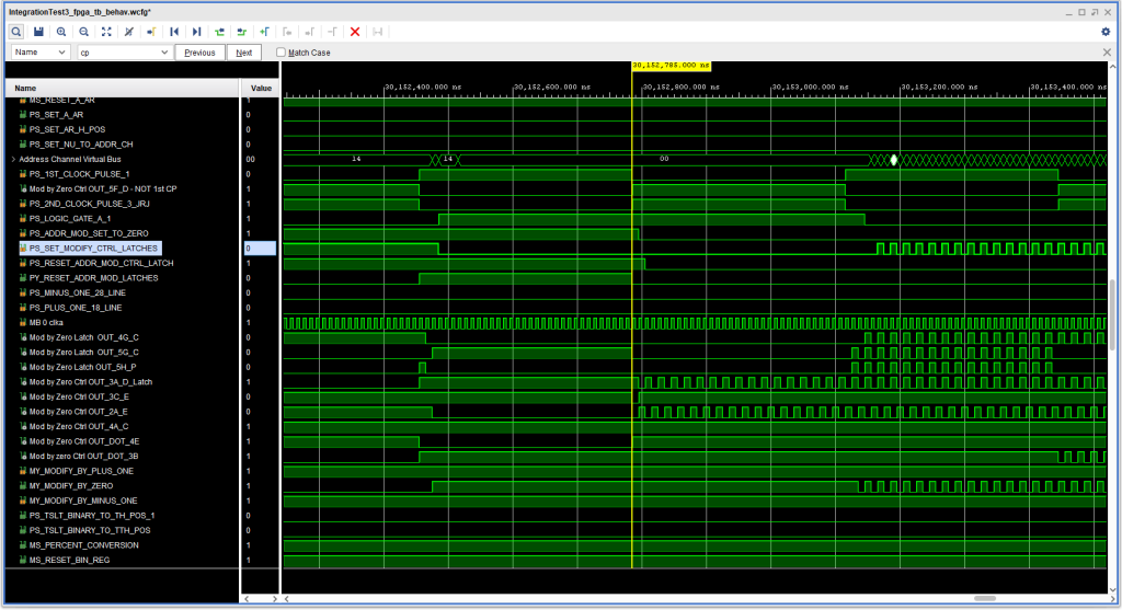
IBM 1410 1401 SAR Instruction Set / Reset Race with ‘9’s in 10K-40K
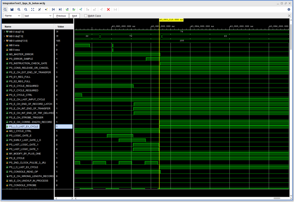
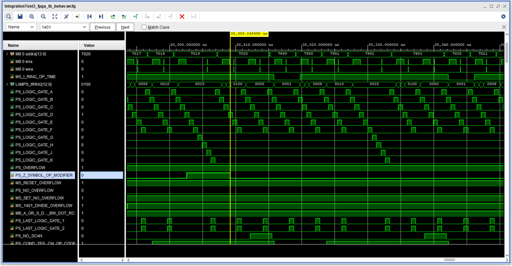
Looking at the timing diagram one can see signal -Y MODIFY BY ZERO essentially “oscillating” starting shortly after 30.153 milliseconds. That in turn caused the Ten Thousands position to change quickly, resulting in the issues as that position is used to select among the B character registers from memory. That latch “oscillation” then in turn set up problems all over the place, particularly in the Address Channel.
Looking again at the same timing diagram, one might notice that +S ADDR MOD SET TO ZERO and +S RESET ADDR MOD CTRL LATCH are both active when +S RESET ADDR MOD LATCHES becomes inactive. Those two signals both impact the Modify By Zero CTRL latch at blocks 3A and 2A of ALD page 14.30.09.1, resulting in the signals trying to simultaneously set and reset that latch – a pair of cross connected NAND gates – a typical R/S latch. This is a big nono.
In my ALD page generation, these latches are recognized, and “D” flip flops are added after each gate involved. So instead of being undefined, in this kind of situation a kind of “oscillation” is set up at about 1/2 the FPGA clock speed of 100MHz (which is also the memory clock signal “MB 0 clka” in the diagram).
The general approach I took to fixing this was to either a) prevent a set during a time when the reset signal was present or b) prevent a reset during a time when the set signal was present.
To try the first approach, I added the +S ADDR MOD SET TO ZERO signal as an input to get logic block at 3C on page 14.30.09.1. This was done directly in the VHDL – much quicker than puzzling out where to find/fudge a logic block to add to the equation and test – especially if, as in this case, the fix doesn’t work. So, apparently this situation really needed to do a Modify Address by Zero operation (which it did: this, like the previous problem, occurred while copying the contents of the A Address Register to the B Address Register.)
So, then I went to the other approach, (undoing the first one), which was to add the +S ADDR MOD SET TO ZERO signal in so as to inhibit a reset while it was active. That indeed fixed the problem, and the change to the ALD was very easy: all I had to do was add the +S ADDR MOD SET TO ZERO signal into the existing “wired OR” at ALD coordinate 4E, as “ECO” JRJ004.
As for the original 1410 implementation, this could easily be another case where the fast FPGA logic causes an issue that never cropped up in the real hardware.
After doing this, the diagnostic worked OK except for the ERR ?3S. (I have not yet tried the manual part of M011 – testing the sense switches, etc.).
Having fixed the 1401 Store B Register instruction and gotten further in the 1410 1401 mode diagnostic program M011, it was time to look at the Store A Address Register (SAR) instruction again.
The CE Instruction materials say:
“Therefore the A address left from the previous operation must move to the BAR before the new A address reads in. This is done during a B cycle that occurs just after the Q-op is detected at I-op time.”
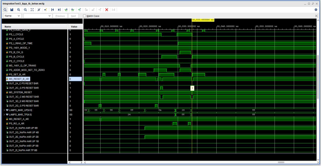
The first timing diagram, below shows that the +S RO A AR signal that presumably ought to be making the AAR contents available becomes inactive before the BAR is reset, so the BAR never receives valid contents – it ends up with invalid binary zeros. (In the 1410, the address registers contain 2 out of 5 code – and having no bits set at all is invalid.) The result was a number of errors, halting the CPU, as would be expected – B Channel, Address Channel, and B Character Select (because the resulting memory address was invalid, none of the 10K “core” modules was selected.
Timing diagram showing issue reading out A Address when setting B Address
There is a signal which looks like maybe it was intended to force the readout of the A Address Register – -S 1401 Q OP TRANS, however once the B cycle starts, the B Character register was cleared and so the signals that relied on – the “Q” character with at wordmark were no there once the B data register was reset early in the B Cycle.
This does not seem to be a race condition. Rather, I suspect it is resulting from the fact that some of the pages for the signals involved are for a 1410 with the accelerator feature, and some without. My hunch is that on a 1410 with the accelerator feature, all of the needed activities to copy the AAR to the BAR occur during the I OP cycle, driven by the -S 1401 Q OP TRANS signal. However, when I tried to force it that way, I was not successful.
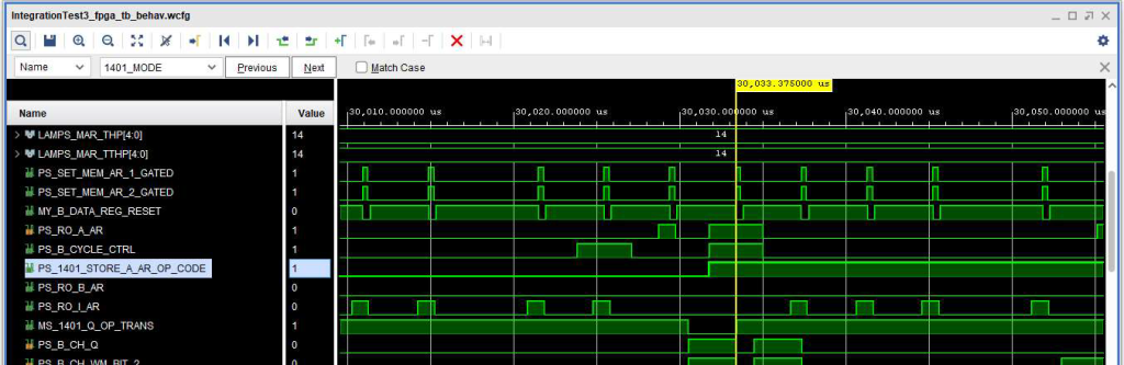
To work around the problem, I added logic to ALD page 14.71.30.1 (A Address Register Readout) to read out the AAR when signals +S 1401 MODE 1 AND +S STORE A AR OP CODE AND +S B CYCLE CONTROL are all active. The result was the timing diagram below (sorry that it is only half of the signals, but the important ones are there.) With that change, the +S RO AAR is active through the necessary part of the B Cycle so that the contents of the AAR are properly transferred to the BAR.
Timing diagram showing fix to page 14.71.30.1 to read out AAR when setting BAR during B Cycle.
With that fix in place, the diagnostics mostly run but fail with console error message “ERR 601J”. So, on to the next fix…
With the 1410 mode CPU running correctly, it was time to test out the 1401 side of things. The 1410 has a toggle switch, allowing the CPU to run as an IBM 1401 compatible with most 1401 programs. The 1410 and 1401 are similar, architecturally. The biggest difference is that the 1401 uses 3 character addresses, with the zone bits over the units and hundreds positions in order to address up to 16,000 characters, whereas the 1410 uses 4 character addresses, capable of addressing memory up to 100,000 characters.
The primary 1401 diagnostic is M011. Once I figured out a problem involving the 1401 addressing scheme, I turned my attention to the next failure: The Store A Address Register (SAR) instruction died a horrible death with B Channel, Address Channel and B Character Select Errors. That problem manifested as a failure to copy the A Address Register to the B Address Register for storing later. I tried for a bit to fix this first, but was not immediately successful, so I decided to try and NOP out the uses of SAR, that mostly had to do with storing the address of each test so it could print out a failure message.
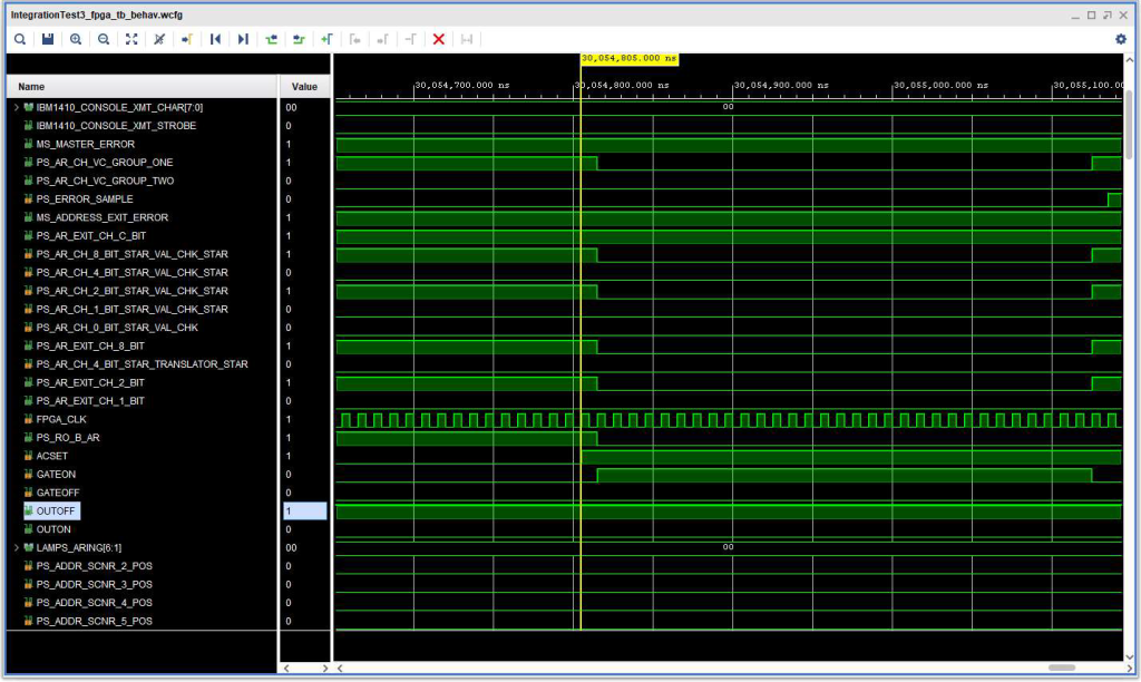
Having done so, the next problem quickly cropped up: the partner instruction for the B address register, Store B Address Register (SBR) also failed – it is essentially the same as SAR, but without that first step of transferring the AAR to the BAR. And the failure error was different as well: an Address Chanel Exit error. The ALD for this circuit is 18.14.02.1 . The ILD is on figure 59 at coordinate 2B – however there is also an error in that ILD. It shows the GateOff input to trigger DEZ as ground (the usual ground symbol). However, on the ALD, the F input it connect to M, which is -12 Volts, and in my scheme, that is logic 0. (Logic 1 being 0V).
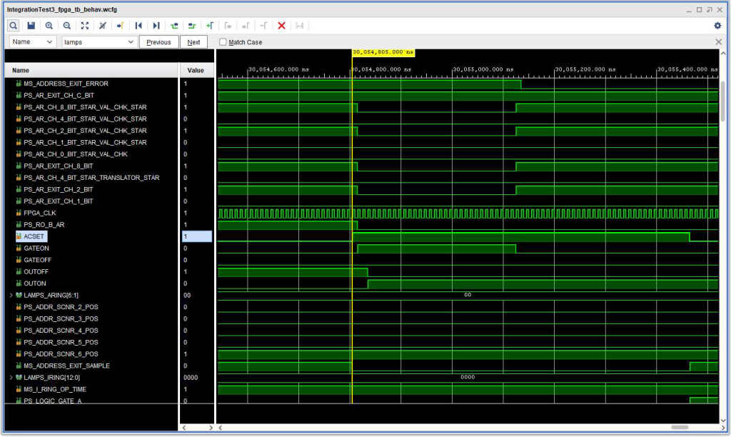
The timing diagram below shows the timing issue. The B Address Register read out and validity check look like they are OK with respect to the Address Exit flip flop ACSET signal. However, the problem was that the VHDL for implementing the SMS card type DEZ has a 3 clock cycle “silo” for ACSET, so that the flip flop is not really set until 3 clock cycles after its ACSET input. In addition, there was no such silo for the other inputs. This silo was put in place to give the ACSET signal some noise immunity – so that a 1 cycle glitch would not set the trigger. But the fact that the other inputs did not have a silo meant that they were sampled 3 clock cycles (FPGA_CLK) after ACSET, and by that time the B Address Register Readout signal (PS_RO_B_AR, i.e. +S RO B AR) had become inactive.
Delay in the Address Exit Check inputs with respect to the readout of the B address Register, resulting in an Address Exit Check.
The relevant VHDL looked like this:
   SMS_DEZ_PROCESS: process(FPGA_CLK, ACSET, DCSET, DCRESET, DCRFORCE, DCSFORCE)
        begin
        if(rising_edge(FPGA_CLK)) then
           if(DCRESET = '0' OR DCRFORCE = '1') then
              OUTOFF <= '1';
              OUTON <= '0';
              SSTAGE1 <= ACSET;
              SSTAGE2 <= ACSET;
              SSTAGE3 <= ACSET;
           elsif(DCSET = '0' OR DCSFORCE = '1') then
              OUTON <= '1';
              OUTOFF <= '0';
              SSTAGE1 <= ACSET;
              SSTAGE2 <= ACSET;
              SSTAGE3 <= ACSET;
           else
              SSTAGE1 <= ACSET;
              SSTAGE2 <= SSTAGE1;
              SSTAGE3 <= SSTAGE2;
              if(GATEON = '1' AND SSTAGE2 = '1' AND
                SSTAGE1 = '1' AND SSTAGE3 = '0') then
                  OUTON <= '1';
                  OUTOFF <= '0';
                elsif(GATEOFF = '1' AND SSTAGE2 = '1' AND
                  SSTAGE1 = '1' AND SSTAGE3 = '0') then
                   OUTOFF <= '1';
                   OUTON <= '0';
               end if;
            end if;
        end if;
        end process;
Once I realized what was going on, the fix was pretty easy. Just add a 3 clock silo for the inputs as well as ACSET. I took the conservative approach, however, and created a separate special instance of SMS_DEZ.vhdl, called SMS_DEZ_SYNC.vhdl to use in the Address Exit validity check logic. This new implementation of DEZ would probably work fine across the board, but I am just using it in the one place, for now.
The timing diagram below shows that now the OUTON signal does not activate – no Address Exit Check, because now the inputs are sampled at the same time as ACSET, and those inputs are still active from the B Address Register readout.
Timing diagram for 1401 mode SBR after fixes.
The relevant VHDL looks like this, for gate type SMS_DEZ_SYNC:
    SMS_DEZ_PROCESS: process(FPGA_CLK, ACSET, DCSET, DCRESET, DCRFORCE, DCSFORCE)
        begin
        if(rising_edge(FPGA_CLK)) then
           if(DCRESET = '0' OR DCRFORCE = '1') then
              OUTOFF <= '1';
              OUTON <= '0';
              SSTAGE1 <= ACSET;
              SSTAGE2 <= ACSET;
              SSTAGE3 <= ACSET;
              GON1 <= GATEON;
              GON2 <= GATEON;
              GON3 <= GATEON;
              GOFF1 <= GATEOFF;
              GOFF2 <= GATEOFF;
              GOFF3 <= GATEOFF;
           elsif(DCSET = '0' OR DCSFORCE = '1') then
              OUTON <= '1';
              OUTOFF <= '0';
              SSTAGE1 <= ACSET;
              SSTAGE2 <= ACSET;
              SSTAGE3 <= ACSET;
              GON1 <= GATEON;
              GON2 <= GATEON;
              GON3 <= GATEON;
              GOFF1 <= GATEOFF;
              GOFF2 <= GATEOFF;
              GOFF3 <= GATEOFF;
           else
              SSTAGE1 <= ACSET;
              SSTAGE2 <= SSTAGE1;
              SSTAGE3 <= SSTAGE2;
              GON1 <= GATEON;
              GON2 <= GON1;
              GON3 <= GON2;
              GOFF1 <= GATEOFF;
              GOFF2 <= GOFF1;
              GOFF3 <= GOFF2;
              if(GON3 = '1' AND GON2 = '1' AND GON1 = '1' AND GATEON = '1' AND
                SSTAGE2 = '1' AND  SSTAGE1 = '1' AND SSTAGE3 = '0') then
                  OUTON <= '1';
                  OUTOFF <= '0';
                elsif(GOFF3 = '1' AND GOFF2 = '1' AND GOFF1 = '1' and GATEOFF = '1' AND
                  SSTAGE2 = '1' AND SSTAGE1 = '1' AND SSTAGE3 = '0') then
                   OUTOFF <= '1';
                   OUTON <= '0';
               end if;
            end if;
        end if;
        end process;
With that out of the way, I could run M011 diagnostics quite far into the tests, until it needed to use the SAR instruction for more than just tracking the test address.