Q: When is a Capacitor not “just a capacitor”

A: When it is acting as a simple delay line

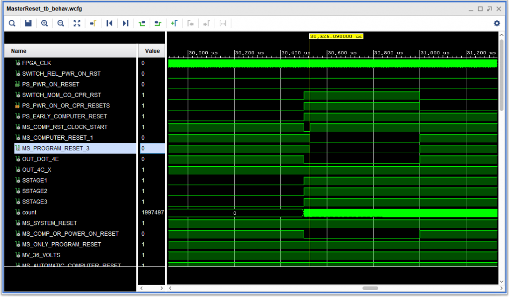
While working on ALD page 12.65.01.1, which generates power on and computer reset signals, I noticed something that didn’t look quite right. The computer reset signal (active negative) when negative when the button push was simulated, then went back inactive, then went active again 25 microseconds later – when it was actually supposed to go active (the result of the timeout of a 25 microsecond single shot gate).

Puzzling – the logic all looked fine. What was going on? At first I thought, “so what – it is going to reset anyway — so no big deal”. But then I looked at the IBM 1410 system fundamentals document, S223-2648, page 26, which makes it pretty clear that the computer reset signal should only be active after the computer reset clock start single shot times out, indicating that the logic gate should stop at either state A or state R. But why?

Then it hit me: CORE STORAGE. If one resets the machine at the wrong time – say, in between reading a character from core (which is a destructive operation) and writing it back, bad things would happen. — the character would be erased. But, how did the actual machine avoid this problem? Sure, I have a relatively long (90 ns, with a 100MHz FPGA clock) single shot setup time to detect the rising edge of an asynchronous trigger on the single shot, but regardless, that setup time would not be 0.

Then I saw it: A 0.047 microfarad capacitor in the ALD page 12.65.0.1 between that computer reset signal and logic ground. Ah HA! A delay!

Fortunately, I had already learned how to implement a delay on an FPGA: with a “bucket brigade” delay line – whose length determines the delay. Sticking a 4 cell (120 ns) delay at that point in the circuit fixed things up just fine.

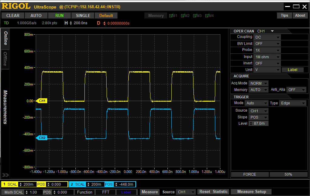
The results are shown in the simulated ‘scope trace, below. (The count signal and SSTAGE# signals below are for a different 20 millisecond single shot.)

A couple of errors in the IBM 1410 System Fundamentals manual

For starters, I should say that the IBM Field Engineering Instructional materials, which I relied on heavily when creating my IBM 1410 Simulator software are excellent, especially considering these documents were typeset in more than a decade before anyone had heard of a word processor.

Nonetheless, I stumbled into two errors in the IBM 1410 System Fundamentals manual, S23-2589, this week. Both are instances where the output signals from gates are different from what is shown in the document.

The first one I ran into was the first Single Shot that I came across in the diagrams, SMS card type DHE, part number 370262. The timing diagram shown in figure 110, page 93 of the manual shows a negative going input pulse triggering a positive going output pulse. An analysis of the electronics in the first of two SMS card manuals (which have no number) and the use of this card in an ALD, 12.60.20.1, makes it apparent that a negative going incoming pulse creates a negative going output pulse. (This was implemented in my FPGA VHDL generation by triggering a counter on the leading negative going input pulse, which then counts down to 0.)

The other error applies to card type DFZ (and its companion, DGA), which I ran into on ALD page 12.61.13.1. The timing diagram in figure 107 on page 92 of the System Fundamentals manual shows NAND logic: If both inputs are high, the output goes negative. However, analysis of the circuit for DFZ, part number 370241 makes it apparent that it is actually NOR positive logic: If either input is high (approximately 0v), then the output is low. Only if both inputs are low (negative voltage) is the output voltage high. This was “sussed out” by looking at the intended logic on the ILD.

The first missing IBM 1410 ALD Sheet

Ran into the first case of needing to reconstruct an Automated Logic Diagram (ALD) page, as part of my ongoion IBM 1410 FPGA implementation project.

The page for the 2nd and 3rd Scan Controls, 12.30.04.1, was missing from my diagram set. I did have information about how many gates from which cards were present on the diagram, gleaned from the card location charts. Fortunately, the Instructional Logic Diagrams (ILD) covered the missing page. Between the two I was able to construct the page, using the original gates, and other than logic block placement on the printed sheet, I expect it is pretty accurate.

I only hope all of the missing pages are so “easy”. Easy is in quotes because on the 3rd Scan Control latch, there is a collector pullover to logic 1 to reset the latch that is not common. That same situation exists with the same card type (DFA), so I was able to verify the gate utilitzatin.

IBM 1410 ALD Volume II Completed

I have reached a sort of milestone in my efforts to replicate the IBM 1410 Data Processing System in an FPGA. The Automated Logic Diagrams (ALDs) comprise 11 volumes – I through XI. Volume I is power supply and general items, and so does not play into the process very much.

The milestone is that I have completed generating and running HDL test benches on all of the pages in Volume II (except for one, having to do with a clock, which is not critical, and may or may not be addressed later.)

I really am surprised about a couple of things. First, while I have fixed a smallish handful of bugs in the data gathering / HDL generation application, there really have not been very many problems in that area. The second is that, aided with the information in the Instruction Logic Diagrams (ILDs) in my testing, I have found very very few issues with the data that was actually captured – relatively few “clerical errors” – few enough that I am pretty surprised.

On to Volume III!

Instructional Logic Diagrams and Automated Logic Diagrams

As part of my project to create a Field Programmable Gate Array implementation (FPGA) of the IBM 1410 Data Processing System based on Automated Logic Diagrams (ALDs), I decided to look at using the Instructional Logic Diagrams (ILDs) to guide my testing, rather than using the ALDs directly.

The ILDs are written completely in “positive logic”. Going in, I sort of expected a pretty imperfect match – that the ILDs would not have all the signals, and be somewhat superficial in their treatment of the logic. For the IBM 1410, the circuits were:

  • AND
  • OR
  • Inverter
  • Indicator (Lamp)
  • Single Shot
  • Latch (Reset/Set)
  • Trigger (Flip Flop)

To my surprise I found that the ILDs are very accurate, and a great testing guide, providing a second view of the logic – a kind of redundancy check against my entry of ALD data into my system. They are good enough that they have given me considerable confidence that I can use them to help “fill in the blanks” related to the handful of ALD pages I am missing, and also for some of the IBM 1414 peripheral controllers for which I do not have ALDs.

Updated 6/28/2020, I discovered that not all of the ALDs are represented in the ILDs. I also had an interesting case where I thought, for a while, an ALD and the ILD that represents it were mismatched, but I was incorrect – the ILD matched the logic perfectly.

In 1962 IBM published an article in the IEEE Transactions “Information Processing — from Engineering Drawing to Manufacture” by R. K. Grim that describes how the data the ended up generated ALDs was entered and the ALDs produced, but it does not mention where the ILDs come from. They are definitely artwork – not machine generated per se. The article did not address ILDs.

I have corresponded with IBM to see if they might have, in their archives, the data from these 1960s era engineering systems, but it seems that they do not (or have lost the pointers to them.)

It seems that the SMS automation was first done using an IBM 709, then they later added IBM 7090 and IBM 1401 systems (which of course could not have been there for the original design of the IBM 7090 and 1401, which used the SMS system), using tape files. The article also describes future plans to use a 1301 disk drive attached to an IBM 1410 for remote (tele-processing) access (which was supported by the IBM 1410-PR155 operating system.

The accuracy of the ILDs is such that I expect that they evolved along with the design of the machine and entry of the data used for the ALDs. I’d expect that doing it after the fact, from the ALDs, would be quite error prone — besides the one difference I have found is in the signal names, which do not always exactly match those used in the ALDs, but are close enough that the intent is obvious. But I don’t know the timing: which came first — the ILDs or the ALDs, or did they perhaps begin together in some form and co-evolve?

In summary, it seems to me that one could do a pretty decent positive logic implementation of IBM machines of that era using these ILDs. This was a real eye-opener.

IBM SMS Generation Application

A lot of development of the IBM SMS data collection / HDL synthesis application has occurred over the past couple of weeks. Recent posts discussed generation of the IBM 1410 oscillator and main logic clock, and the I Ring – the instruction readout ring.

The application now supports Lamps, as well.

Also, the application now supports gathering signals into an HDL bus for economy of representation. Bussed signals are defined in a database table which translates an individual signal name to a bus name and which bit of the bus it occupies.

Update 6/20/2020: In this most recent week, support for switches has also been completed.

Update 6/27/2020: In this most recent week, I added the capability import information from a CSV file describing “bused” signals to create HDL bit vectors.

IBM 1410 FPGA Simulation – The Brainstem

Additional work has resulted in another step forward in my efforts to reproduce the IBM 1410 (in particular, the IBM 1411 CPU component) in an FPGA.

I now have pages 11.10.0*.1, 11.10.10*.1 and 11.10.20*.1 generated and tested (see the image, below).

One very hopeful sign is that easily 90% of the effort in the last couple of days was enhancing the application to preserve a section of VHDL declarations in a test bench, and debugging VHDL test bench code. The generated HDL had performed nearly flawlessly.

In the image below one case see the following (MS… signals are a translation of -S IBM signals – active low. PS are +S – active high.

  • The simulated 100 MHz FPGA clock
  • The 1.5 MC (MHz for you modern people) system oscillator
  • The two phase system clock pulses
  • A test bench provided MS_PROGRAM_RESET_3 signal, provided by the test bench.
  • The logic ring gates A through K and R through W. The latter are only active in the last part of the test, and represent an overlapped I/O request (cycle-stealing, if you prefer)
  • A test bench provided PS_LAST_LOGIC_GATE_1 signal – telling the logic gate ring that it can go back to the initial “A” state.
  • A non-overlapped I/O cycle request (E Cycle means a cycle taken for the first, or E channel – not to be confused with logic gate E)
  • An overlapped I/O cycle request on the first channel
  • The PS_COM_DISABLE_CYCLE which “freezes” the logic ring – overridden by the non-overlapped E cycle request.
IBM 1410 Logic Gate Ring Simulation
A Xilinx Vivado simulation of the IBM 1410 Logic Gate Ring

The FPGA Simulated IBM 1410 has a “pulse”

Having spent the past few months cleaning up my IBM 1410 SMS database program, and posting it to github at https://github.com/cube1us/IBM1410SMS , I have spent the past couple of weeks focused on the HDL (currently VHDL) generation, using GHDL and Xilinx’s Vivado toolset, with an eventual destination of my Digilent Nexys4 FPGA (Field Programmable Gate Array) board.

After fixing a few bugs, and implementing the oscillator (by way of a counter/divider from the 100 MHz FPGA clock), I loaded the results into the FPGA, and as show below, my IBM 1410 now has a clock, running at the right frequency for an IBM 1410 with the accerated throughput feature, as shown below:

IBM 1410 FPGA Clock
IBM 1410 FPGA Clock

On the original machine the lower signal, on channel 2 of the oscilloscope, was derived from the first using a delay line – about 330 ns of delay. Kinda hard to do with an FPGA. 😉 So, I implemented delay lines using a series of flip flops clocked by the 100 MHz FPGA clock – so, in this case, there are 33 of them.

This signal is not simulated – it is a real signal that exists in the FPGA.