Having fixed the problem with the space, I continued to test out the IBM 1410 in 1401 mode. At first, I had thought that it was getting quite far in the diagnostic M011 – it would error out with the I register (instruction counter) at 6029. I spent the better part of a day chasing down an apparent problem with the Store A Address Register (SAR – opcode Q) instruction at the indicate location. However, when I placed a halt at the test before that, it still failed at the same place. How could that be?
So, I decided it would be worth the trouble to run the 1401 diagnostic in Instruction Fetch/Execute mode (I/E). The problem became apparent much more quickly than I had anticipated. After halting at the halt and branch instruction at location 2018, it ended up trying to fetch an instruction at a location near 06020. (My memory is just a little fuzzy on when that flying leap actually occurred, and I don’t have the output anymore.)
As you may know, the 1410 has 5 digit addresses, whereas the 1401 used 3 digit addresses plus zone bits to address up to 16K of memory. It was clear that somehow the translation from the 1401 style address to the 1410 address register had gone awry.
A little digging reminded me that there was one page of the automated logic diagrams (ALDs) associated with this translation, part of what is called the “Zone Adder” that was missing – page 14.18.04.1. After some time working with the xsim simulator under Vivado, I began to suspect a problem with my re-creation of the logic from that page.
Input “A”: -S ZONE ADDER A A DOT B A
Input “B”: +S ZONE ADDER B BITS EVEN
Output “O”: +S A NOT A DOT B A DOT B BITS EVEN
The output name is sufficiently complicated that the equation for this is not self-evident. Looking at the ILD figure 55, it looks like the following should be the equation:
O <= NOT A and NOT B — The NOT A is because A, above is -S not +S
Interestingly, page 14.18.04.1 is not referenced at all in the 1410 1401 Compatibility manual on page 7. On both the ILD and that manual, this signal is routed to the middle of a logical OR gate labeled “Zone Adder Carry”, which is laid out on page 14.18.06.1.
Regardless this VHDL caused the problem noted above. However, I had also penciled in on the ILD an additional inverter, which would be the signal without the added inverter (double negative and all that…). For that, the equation would be:
O <= NOT(NOT A and NOT B)
And it actually takes one less “fudged” gate, because the SDRTL provides this result outright.
It turns out that removing that inverter from the logic for that ALD (and thus implementing this second equation) cured that particular problem, both under xsim and running on the FPGA. But, at least superficially, this makes it look like it does not match the ILD — at least at first.
However, and finally, examining the page to which this signal is routed, 14.18.06.1, one sees that it is routed to a logical OR (physical NAND) gate where -S / -B active inputs generated the +S active output. So if one takes the two together, the end result is such that it does match the ILD.
The diagnostic didn’t get very much further, however, and now fails at location 2032 on a SAR instruction, similar to the failure after the “flying leap” problem, just at a different location. SAR is interesting in that it first copies the A Address Register to the B Address Register, and that is apparently failing.
No, not that kind of cadet. Unlike the IBM 1620, the IBM 1410 does have adder circuits for doing addition (and multiplication and division as well). Instead, this issue had to do with the IBM 1415 space function.
I had thought that the principle instruction diagnostic, CU01, was working perfectly, but it was not quite so. I had noticed that even after finishing the diagnostic, I kept getting space characters sent to the PC support program, but figured that was just a software bug somewhere. However, when I started to run IBM 1410 1401 compatibility diagnostic M011, it stopped typing its instructional message to switch to 1401 mode on the console when it hit the first space character.
After some sleuthing, I discovered that the console typewriter logic never asked the channel for the character after the space – it just kept sending that space to the console typewriter again and again and again.
As one might expect, the issue turned out to be in the console typewriter Selectric emulation VHDL code. I had miss-interpreted the signal -V CON PRINTER SPACE NO to just involve console input via the space bar. a closer look at the related automated logic diagrams (ALDs) made me realize that in fact this was also the Selectric’s way of telling the 1411 that the space process had been completed, and that it really had nothing to do with input from the space bar.
At first I tried to just use the relevant states of the finite state machine (FSM) that controls spacing. That did not work right, however, because that same FSM also controls back-spacing. Qualifying the logic signal to only be active during a space, but not backspace, operation filled the bill.
With the console typewriter working, and the ability to load core images, I was now ready to try and run some diagnostics. The first issue I ran into was that the main diagnostics, CU01, was initialized for 80K of core. That the core image file was larger wasn’t an issue: the Windows based support program knows to only send the first 40K. However, there was a flag denoting machine size that needed to be “patched” — which I did using my emulator, and then saved as a new core image.
Loading the diagnostic, it typed out its identifier, but then quickly errored out with an Assembly Channel error on a Subtract instruction where the destination B-field was initially positive, but turned negative during the subtraction. This was not the first place I expected to see an issue – figured it would more likely relate to some trigger or other. But nope, this was a simple issue in the Assembly Channel.
The problem arose because the ALD diagrams I have are mostly for an IBM 1410 with the Accelerator special feature, however, most of the ALD diagrams for the Assembly channel proper (ALD 15.50.xx.1) are for the non-accelerated version whereas the Assembly channel controls (ALD 15.49.xx.1) are for the accelerated version. There were several signals that ended up either not being used, or having no source as a result:
-B B CH MIN+INV PLUS SIGN GATED
-B B CH PLU+IN MIN SIGN GATED
-B B MN +IN PL+PL+INV MN GATED
These all relate to cases where the B field ends up with a sign other than its original sign. I suspect that the idea was that these signals provided earlier gating to the assembly channel rather than just deriving them from the adder with additional gate delays.
After fixing the Subtract issues which involved just the “B” bit on page 15.50.06.1, (going from positive to negative) I immediately ran into the same issue on the first pass of the diagnostic during the same test, changing from negative to a positive result. Fixing this involved pages 15.50.05.1 (mostly). As a result the pages for the Assembly channel have some gates who’s note at the top is “FUDGED”. 😉
With that, so long as I didn’t enable I/O overlap and Priority Alert (interrupts) during the test, CU01 completed successfully! Frankly this was something of a surprise: It tests most of the instructions and ways of moving data and they all just worked.
Also, the run time of about 3.75 minutes matches very well with the information in the diagnostic listing for a 1410 with the Accelerated logic feature.
So then, I ran it again, but with overlapped I/O and priority features turned on in the diagnostic. It ran fine for about a minute, but then failed during overlapped execution of a multiply instruction. More on this during the next installment.
The IBM 1410 FPGA project has reached a milestone. Console input of characters, word mark, space bar, index (force premature end of line) and the special inquiry keys: request, cancel and release is now complete.
With that it is possible to display memory, update memory, start execution at a specific address, start the machine, stop and machine, etc.
I have tried a few instructions in as simple way: Set Word Mark, Halt, Add, Subtract, Jump on Inquiry Request and Jump unconditionally, and they work OK for at least a very simple example.
With this, the implementation is very close to being in same state as a real IBM 1410 donated by Oscar Mayer that we played with in the basement of the University of Wisconsin Computer Science lab: CPU, console but no peripherals or I/O synchronizers.
There are some issues, though, both with the console implementation and with the FPGA implementation. For the FPGA
The Console Check Test 3 fails to set the ADDRESS CHANNEL error. This is a “fight” between the DC Set which the switch activates, and another signal holding the trigger reset. (I think an earlier blog post discusses this in more detail).
Attempts to display memory at 09998 show only two characters (this may or may not be correct), and attempts to display memory above 10000 fail miserably with a B Character Select error. This could be an issue of a gate being present that should not be, because I generally entered all gates using the IBM 1410 SMS application, even ones that I knew I would not want eventually, and/or a missing tie-down or tie-up of a signal. This is a critical problem to ferret out and fix. [Resolved 6/11/2023 – simply a matter of marking most of the gates for features “S10” (or $10 depending on where you look) and “S20” for “no generation”.]
As mentioned in an earlier post, when starting a display memory sequence, during the first step – address entry – a “D” should be displayed. Instead an underlined (invalid parity) “F” is displayed because of a bit 2 “pick”. This looks to be an error in the actual ALD, will be easy to fix, but doesn’t really affect much of anything.
An attempt to do output I/O to the console, using instruction M%T0aaaaaW does not operate properly — it repeats the first character in the I/O buffer at address “aaaaa” without end. This is also a critical problem, as diagnostics need to do this. [This has also been fixed as of 6/20/2022. It might have involved the change that *removed* a “D” flip flop after gate 3F.] [Update: This problem has also since been resolved.]
With the addition of the console, there are now three github projects involved with this effort:
Since the last post, I have begun working on inputs – switches, in particular. The input subsystem is much simpler than output, at least for things like switches and console input- there is no need for any kind of common FIFO or arbitration. Instead the module IBM1410_UART_INPUT_SUBSYSTEM receives data from the FPGA development board UART, and then places that character onto one of N (currently 0..7) input FIFOs (one each for receiving data for switches, console input, card reader, and so on), and N write data flags.
Then, each input module (for example, module IBM1410_CONSOLE_SWITCHES_RECEIVER) reads data off of its FIFO, and does the appropriate thing with that data. Specifically for switches, this means receiving the entire vector of switches into a temporary vector, and once fully received, replacing the one that the 1410 itself is using.
Testing the various switches has led to some interesting discoveries:
Adding switches made a number of multi-page combinatorial loops pop up, that were previously hidden as a result of optimization by the Xlinx Vivado toolset. The 1401 compatibility switch was the second (and I hope last) of the loops involving large numbers (more than 300) gates. I could have change the design rule check to ignore this issue, but I decided instead to modify the SMS generation application to look in the logic block Notes field for “DFLIPFLOP” causing it to add a D Flip Flop after the identified logic block.
I like to be able to run the FPGA CPU on its own. This means that it’s initial switch vector (the one that gets copied into when an entire switch vector is received from the host support program) needs to be reasonably initialized. To do this there are a few SWITCH_VECTOR(….._INDEX) => ‘1’ entries along with an OTHERS => ‘0’ at the end to set things up right. This fact is what actually led to the replace with a buffered copy concept described above. (The first time ANY switch is activated on the PC host program, the entire switch vector gets replaced by the transmitted one; indexing in hardware is hard. 😉
While testing the “DISPLAY” function of the console’s MODE switch, when one presses START, a “D” should appear. However, currently, instead an “F” with invalid parity currently appears. This is occurring because the printing of “B” is also enabled, causing a “pick” of the “2” bit. It looks like my ALD is out of date – the “B” should really be being suppressed under these conditions – in other words, a hardware “bug”. Sure hope there are not too many of those! A similar thing happens with the MODE switch set to C.E. A “#” should be printed, but instead I get a “.” – same bit pick, for the same reason.
Pressing CHECK TEST SWITCH #3 (and holding – which the C# user interface host program makes easy by holding on a click, and then releasing on the next click), and then pressing START should light up all the PROCESS CHECK lamps. This works fine for check test #1 and #2, but for #3 it does not light up the ADDRESS CHANNEL error as expected. This scenario uses the DC SET input to set the flip flop, but it appears that there is a signal using collector pull down causing the flip flop to reset (DCRFORCE in the SMS gate’s module) at the same time – and that reset it taking priority in the VHDL. There are not too many of that particular gate type in the system, so I may try reversing the priority of those things, so that a DC SET takes priority and seeing if that breaks anything else.
The SCAN GATE switch on page 14.17.18.1 (part of the ADDRESS STOP circuitry) has a note that says it is a “CIRCUIT OPENINING” switch – in other words, all outputs are -36V except the selected position. In most cases in the IBM 1410, a connected switch means ‘0’, that is, -36V, so this behavior is (to be verified) a natural outcome of how I implemented switches – I “NOT” switches in the VHDL all – because an “on” switch electrically connects to -36V. For this switch, a given unselected position has to be a ‘1’, which is then “NOT-ed” in the VHDL to a ‘0’ – which then forces the output of the gate it is connected to to a ‘1’ – taking it out of the filtering criteria for address stop – it’s scan position can be either on or off. This, along with a failure to initialize the SCAN GATE switch and the address top address switches had me tied up in “NOTs” for a little while (pun intended.)
On this same page there are a couple of optional SYNC COND inputs – at least one of which need to be tied to logic ‘0’ in order for address stop to work. They were intended to give CE’s a way to do an address stop on arbitrary conditions inside the machine.
Having the 1410 sending output to the console a few months back was great, but lots more is left to do. Over the past few months I have been working on a couple of needed capabilities:
The console is only one of many devices that will need to send output out from the FPGA development board to a support application. Others will include lamp display information, tapes, disks, printing and punching. In order to make that happen, I needed to do several things:
There needs to be a FIFO, since at times multiple devices may need to send output to the console support program, and they are not “aware” of each other – they could conceivably overlap in activity. Also, some devices (like lamp output) would not necessarily be constrained to IBM 1410 cycles – they could generate output more quickly. That means that some kind of FIFO is required.
Since devices could possibly send at the same time. There needs to be some kind of arbitration to decide which device has priority and gets to go first.
The arbitration and transfer of a character to send to the support host would not be instantaneous, which means that each device that can generate output needs to have at least a single character buffer, and some kind of signal to tell it whether that buffer is full or empty.
A multiplexor to select which source is currently providing the next character to be placed into the FIFO to send out.
These capabilities were created in VHDL in the module IBM1410_UART_OUTPUT_SUBSYSTEM, which is comprised of up to eight (currently) “requesters” (that one character buffer and flag signal, so one for the console, for now – but eventually more of them), the “arbiter” which decides who goes first, the “mux” (the multiplexor), “mux to fifo” which manages the transfer of characters from the multiplexor to the fifo, and “fifo to uart” which manages the transfer of characters to the UART when the UART is available to send more characters.
I am also in the process of modifying the SMS HDL Generation Application to generate vectors for lamp bits for transmission to the support host program, and switch bits to accept switch information from the host program. The lamp vector will be sent out from the FPGA periodically (maybe as often as 20 times/s) via a state machine to display lights on the emulated console in the support host program, and the switch vector provides a convenient means to number each switch for the purposes of host/FPGA communication.
Eventually there will be a serial input subsystem as well, to support the aforementioned switches, as well as input devices, like the card reader, tape, disk and so on.
The last 12 months I have been pretty busy working on my 1410 in FPGA project, and there is now more to share, though I have not done much actual work since February – been too busy playing with other “toys”. 8D
First, I finished working through all of the IBM 1410 and IBM 1415 Automated Logic Diagrams – generating VHDL and testing the results with test benches. [Note that this includes the built-in 1401 compatibility mode, activated at the flip of a switch.] That took most of 2020.
So, the CPU generation in VHDL is now more or less complete, and I added a hand coded memory module for memory, as core is kind of hard to find on an FPGA development board. 😉 I am currently using a Digilent Nexys 4, but I think it might have even fit on a Nexys 2 – there is plenty of room to spare, and there isn’t anything in the VHDL aside from, maybe, the memory implementation (though even that is pretty generic VHDL).
With this the CPU runs, at the very least, Unconditional branch (Jump), Halt, NOP and Set Word Mark instructions seemingly correctly – I haven’t tried any others. Somewhat surprisingly, aside from issues with the hand coded VHDL in triggers and the need to communicate pins tied to logic one or zero, the auto-generated VHDL works untouched.
I have updated the github repository for the C# database application that generates the VHDL from time to time (and which includes the complete database) at http://github.com/cube1us/IBM1410SMS
There is now a *new* repository, http://github.com/cube1us/IBM1410FPGA which holds the generated VHDL, some hand coded VHDL modules for certain SMS cards (typically for triggers, for example), the console and test benches I used along the way, and VHDL “Integration Tests” which are designed to be loaded onto the board – the current one being IntegrationTest3.
There will be, eventually, a third repository which will contain the C# code that “hosts” the IBM 1410 console and peripherals, communicating with the FPGA over a high speed serial over USB connection. I figured out that this should allow me to emulate peripherals without having to resort to sending data over Ethernet, SPI, I2C or the like. I have just started that, so it really isn’t at a point that there is much to share.
Once I have a console working (which will require a re-do of the console VHDL implementation, which right now communicates in ASCII, but should probably be using BCD), I should be able to pre-load into memory some of the CPU diagnostics, by loading a diagnostic routine into either my 1410 simulator (http://github.com/cube1us/1410), or Richard Cornwell’s emulator in SimH and then taking a snapshot of “core” to pre-load into the FPGA. At that point I expect I will be able to test the CPU pretty thoroughly. I hope and expect that will happen this year sometime.
Unfortunately, I do not have the ALDs (Automated Logic Diagrams) for the IBM 1414 I/O Synchronizers, but I do have the Instruction Logic Diagrams which should allow me to code VHDL to emulate card, tape and maybe eventually even disk functions, so those might take a while.
Getting console output was going to require writing some VHDL of my own – I don’t have an actual IBM I/O Selectric available! I started out by reading through the material in the IBM 1415 Console CE Instruction manual (S223-2648) to design some finite state machines (FSM) to stand in for the console cams and feedback contacts.
The I/O Selectric uses cam contacts to control the timing of things like when the type ball tilt and rotate has completed, when shifts have completed, when spaces and backspaces have completed and when a carriage return has completed. It uses additional feedback contacts to indicate the parity of the received character, whether the keyboard is locked and the current shift state (upper or lower case).
To save time, particularly during simulation, I sped those timings up by a factor of 100. Mostly this just involved the console implementation module itself, via a VHDL generic parameter, but I also had to adjust the single shot on ALD 45.50.01.1 as well.
The Selectric also uses a set of solenoids to initiate actions such as printing a character, locking/unlocking the keyboard, spacing and backspacing, carriage return and shifting from/to upper and lower case.
After writing some simple state machines for the cam timing, I enabled the normal stop print-out in the CPU via a test bench signal, and then used simple VHDL with “wait” statements to check for the outputs and provide the input signals required by the CPU in order to test my understanding under simulation.
The first thing I came across was a latch on page 45.50.15.1 that did not have a reset. In real world hardware this can work because (unless it enters a meta-stable state on power up) it will be in one state or the other. However, under simulation that does not work – it ends up as an undefined signal – so I added a Program Reset signal to the latch at location 4A on that page to compensate.
The next thing I saw in the traces – which I hadn’t expected, but probably should have – was activation of the carriage return solenoid so I had to add the FSM for that. (Note: The I/O Selectric implements a carriage return by returning the type ball to the home position and initiating a paper (line) feed operation).
This was then followed by an “S” character – and the fun began. The interface feedback signals from the Selectric are full of names that end NC or NO (normally closed, normally open). Now one might expect that these refer to the state of those signals at idle, but the cam contacts aside, that quickly got pretty confusing – more so because most of these signals (except those that drive the solenoids) are active low. In addition, the keyboard lock signal is -W on the CPU diagrams, but +W on the 1415 Console Printer contact diagram page 40.30.01.0, and a couple of the feedback signals from the Selectric to the CPU are marked as -B level on the ALD page — but are actually -V level, as can be determined from page 40.30.01.1 as well.
Eventually I came to the realization that the best way of handling the NC vs. NO +/- confusion was to more or less ignore it, and instead use the signal name and level to determine what state a given signal ought to be in at a given time. That helped a lot. Once I got ordinary characters working right, I proceeded to code the state machines for space/backspace, and shifts.
Shifts were a little problematic at first, because the CPU drops the solenoid drive the instant it sees the feedback signal from the Selectric – which didn’t give me a clock cycle to save the new shift state.
Once I got that working under simulation, I turned my attention to getting that I/O from the Selectric to a PC for display. A few months back I had looked into using a MicroBlaze soft CPU to do that, but looking at how my Digilent Nexys 4 USB to PC connection works, I discovered I can run successfully at speeds of at least 115,200 bits/second, which should be plenty enough to run a simple flag bit/type protocol for not only console output, but also switch inputs, printer output, card input, tape I/O and disk I/O – perhaps adding a silo or two for lower priority devices. This is a huge simplification over what I had been thinking would be necessary.
But at this point there was also a little bit of extra work required. initially I had written the VHDL to use character output for the UART, but I subsequently discovered that VHDL doesn’t have a consistently synthesizable way to convert from character to std_logic_vector, so now that type-ball characters are specified as std_logic_vector bit strings, instead of ASCII characters – which is probably better in the long run, anyway. Mostly I am using the same encoding I used from the IBM 1410 simulator software, which in turn was derived from Joseph Newcomers IBM 1401 emulation software.
Once I had tested the UART VHDL, found at Nandland, I put together a test to combine that with the CPU and generate a bitstream for the FPGA. I had two small problems in the process – trivial ones, really. The first was that I keep forgetting to wire signal “+P SPECIAL +12V POWER FOR OSC” (which then feeds “+P SPECIAL +12V FOR REL DRIVERS”) to logic ONE. The second issue was that while most of the buttons on the Digilent Nexys4 are active high, the Soft CPU reset button – which I feed to the 1410 CPU Computer Reset signal is active LOW – wasted an entire day on that one. 8(.
One I did that, I obtained the following result: A printout of:
S 00009 00007 00007 .c … _ _
This is exactly the expected result (one which I had already observed in simulation). The “c” is a 1410 blank (different from the console space operation), and will print as a “b” using a PC-side application. Also, the three periods after that, which are the contents of the A Data Register, B Channel and Assembly Channel, have wordmarks – which you cannot see in the PuTTY output because they get backspaced over. Finally, the last two characters, the channel unit select and unit number registers for Channel 1 are wiped out by the backspace/underscore combination that occurs because they seem to be uninitialized, and therefore have bad parity.
Next on the list will be cleaning up the latches in the VHDL code which are currently tracking upper/lower case, tilt, rotate, space/backspace, and the character to be sent to the UART, and maybe a couple of more, as well as working on the PC side console application – starting with designing the protocol I will use for PC / IBM 1410 communication.
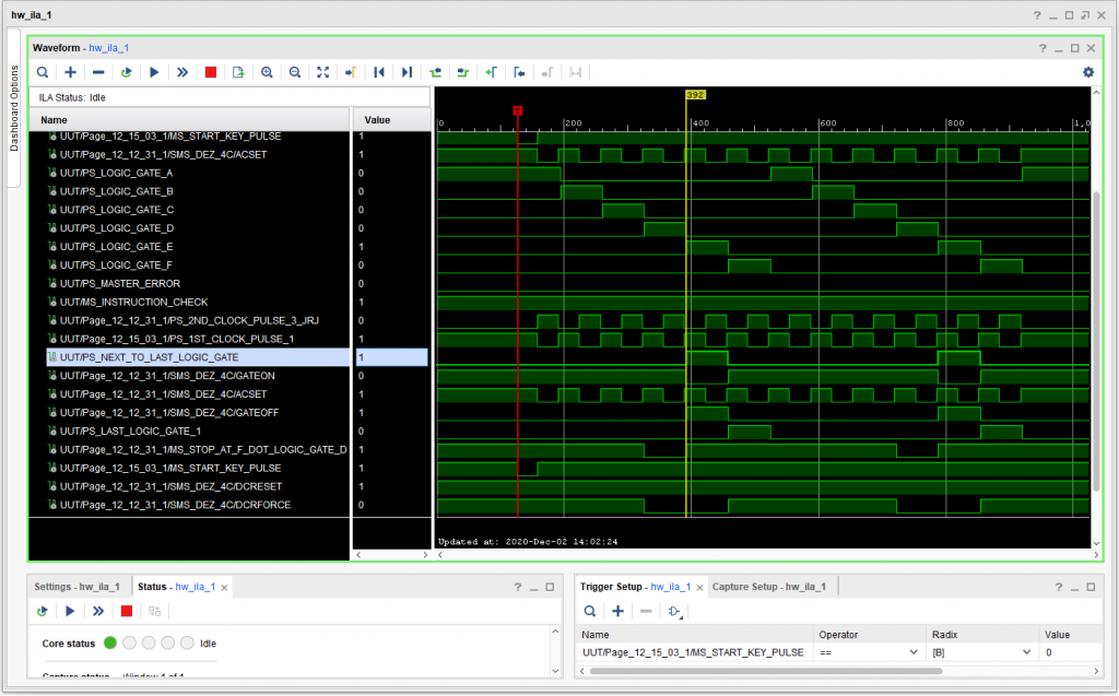
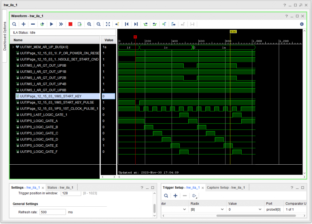
What with the Thanksgiving holiday and all (even though it was spent at home, ’cause 2020), it took several days to ferret out the issue where simulation of a power on reset followed by START worked, but on the FPGA that failed. Of course it was bound to be an issue with triggers. However, I used the Integrated Logic Analyzer (ILA) to confirm that issue before I changed anything. Sure enough, card type DEZ needed the same adjustments as DEY: I changed it so that the transition of the AC SET input was required to occur after the transition of GATE ON / GATE OFF. At the same time, I moved all of that logic inside the FPGA clock transition section, to make it synchronous with the FPGA clock. That fixed the issue, which occurred on page 12.12.31.1
So now, after I load the FPGA, all I need do is press START and I see the correct waveform. (Also note that the transition of the output to ON (NEXT TO LAST LOGIC GATE) immediate turns off GATE ON – because that is exactly how it is wired. So first we see -S (active low) STOP AT F . LOGIC GATE D at about 320 into the trace. Note that GATE ON is already present, however, the trigger is held off by the “DCRFORCE” input coming from block 3B until STOP AT F . LOGIC GATE D goes true. Next, we see CLOCK PULSE 2 appear (but it gets inverted before it us used for ACSET, so it essentially matches CLOCK PULSE 1) at 389 on the diagram. Then at 392, the trigger sets, NEXT TO LAST LOGIC GATE goes true, and GATE ON is removed.
Corrected timing for power on reset followed by START
Decoding Memory Addresses
The IBM 1410 storage address register (STAR) is a five position two-out-of-five code register. However, it is not used altogether to select an address. On a read, all of the 10,000 position core memory segments are read, in parallel, each to its own B data register position. So, for a 40K machine, it has 4 B data registers, for 0-9999, 10000-19999, 20000-29999 and 30000-39999. On a read, the ten thousands position of the memory address is used to select one of the B data registers to gate onto the B Channel. During the write portion of a memory cycle (to change memory, or to regenerate memory if only a read is required), the ten thousands position is used to decide which B data register to update, if any, before the write portion of the memory cycle. The other B data registers retain their original contents from the read cycle.
At present, rather than simulating the full core plane of the IBM 1410, I chose to implement memory, for now, using a binary address and (probably) an array of 10K FPGA Block RAM segments. This means that the binary addressed RAM for the FPGA IBM 1410 uses a 14 bit address (to cover 0-9999), with memory arranged in the same 10K sections.
The inputs into this decoder are the -Y MEM AR UP/TP/HP/THP signals, which are in two-out-of-five code. The output from the decoder is a 14 bit binary address, 0 – 9999. This was implemented “brute force” by decoding each of the positions to the appropriate binary number, so the UP decodes to 0 – 9 in a 14 bit binary number, the TP decode to 00 – 90 (by tens) in a 14 bit binary number, and so on. Then the four binary numbers are simply added together in the VHDL – leaving the implementation of the adder for the tool chain to figure out.
Memory – and a Startup Issue
Next I created a simple set of Block RAM modules (BRAM) along with a VHDL wrapper for the 40K main core unit, accepting the aforementioned addresses in 2 out of 5 code, the Ten Thousands position (so that eventually it can tell if it is the 40K main core or the 60K Z Frame core), inhibit signals, and output sense signals. In order to more easily generate the necessary BRAM enable and write enable signals, I also brought out the MY_X_RD_1 and MY_X_WR_1 signals.
After some fussing I got my BRAM module working under simulation, but ran into an odd problem where during startup the system would overwrite location 00001 with garbage (and presumably 10001, 20001 and 30001 as well) because the system was left in Logic Gate B (LGB) state during the power on reset that then proceeding through a memory cycle once the power on reset was complete triggering the computer reset- thereby writing those locations with uninitialized garbage. (Computer reset will finish a cycle if it is encountered mid cycle to avoid corrupting core.)
I temporarily disabled memory writes, and then found I could successfully execute my halt instruction (WM/. WM/. in locations 1 and 2) under simulation AND on the FPGA.
The startup issue was interesting. I had supposed that the power on reset signal issued on ALD page 12.65.01.1 would start OFF, come ON during the power on reset, and then turn OFF again. However, that was having the undesirable effect of letting the system progress from LGA to LGB during the power on reset as mentioned above. Some study of the aforementioned ALD, along with the IBM 1415 console manual (the power on switch is located there) made me realize I had misunderstood.
That power on reset signal is asserted during power on to keep the system in a reset state (and thus in LGA) for an RC constant of about 500ms. Then, after that, the signal goes to logic 0, triggering the one-shot at block 2D to do a computer reset. At that point, the machine is in LGA, and the computer reset will leave it there.
Since I already have a system initialization VHDL process in the FPGA VHDL logic, it was easy to manage the power on reset signal there – indeed, the two may eventually become one, as they both have the same purpose of getting some stuff set up before letting the IBM 1410 CPU start.
This tested OK under both simulation and on the FPGA, though I have not yet verified that the FPGA is actually writing the contents back into the BRAM.
Next up: testing write by setting a wordmark somewhere (to verify read/write), and then halting, and a simple loop – both of which should be possible with my current VHDL by just changing the RAM initial values.
Update: The instructions sequence, starting at location 1, of setting a word mark at location 8 (which takes locations 1 through 6), a NOP instruction (reading out the set word mark instruction needs a wordmark on the character after) and then a period (halt without the word mark) behaves correctly. Wohoo! I have something of a CPU.
Having completed the pass through the ALDs, the next thing I undertook was some cleanup work. The goal was to be able to generate an HDL “group” that contained ALL of the usable HDL pages.
The first step of that was to mark pages I didn’t want as no HDL generation – a relatively recent addition to the application. Then I went through and found all of the switches, and regenerated the affected pages to use update code that used notations in what is ordinarily the signal level fields of the ALD logic blocks associated with the switches (but show up as thinks like DK 2 – meaning switch deck two of a multi-layer rotary switch). I also had to fix up the associated test benches and groups to use the new signal names.
Then I took a shot at generating the whole shebang. I ran into three issues. There were a couple of pages I had skipped that had to do with auto-restart. Dealing with those was simply a matter of marking them to not generate. Next, I ran into an issue with page 13.72.06.1 – which turned out to be a missing page having to do with compute disable cycles for systems with “fast” file (disk) systems. Finally, the ALDs had several cases where the same IBM 1415 console lamp location was specified. I separated them arbitrarily – I don’t seem to have any specific information to help me decide.
Simulation Begins
With those fixes I was able to begin simulation. At first the power on reset wasn’t working right – the 20ms single shot on page 12.65.01.1 wasn’t triggering. This is really a simulation issue, I think – putting in a 30ns wait at the beginning of the simulation dealt with that.
The next issue was that after the reset, pressing the start key did not start the clock – the STOP LATCH stayed on. That in turn kept the clock from starting (ILD Figure 1). That in turn led to noticing that there was no START KEY PULSE when the start key was pressed in the simulation.
Part of the issue was tracked down to the fact that I don’t yet have a console printer emulation in place, and the console contact signals were inconsistent (both C1 and C2 normally closed and normally open signals were false), so I “fudged” it so the cam contact signals would indicate it was not in a cycle. That helped – and was the sort of thing I expect might need attention.
The next issue with the START KEY PULSE signal was that the CONS STOP PRINT COMPLETE signal was 0 – as though it was in the middle of a console stop print out. That was traced down to the Console STARTPRINT switch (page 44.10.01.1) which is unusual in that its N output (usually reserved for an active HIGH signal) is active LOW in this instance. That got me to the point where the START KEY PULSE appeared, and the machine went from Logic Gate B (perhaps it should have been at A?) through Logic Gate E, and which point Master Error was asserted and things stopped.
The error lamps were multitudinous, but the lamp that was first in line in the time line was the B Register Reset Error. The B register gets the contents from memory, and if it does not reset before then, that is an error (otherwise it might return the previous character, or some combination of the previous character and the current one).
Have I ….
By now, if you have been following along, you know what comes next. Yup. Triggers. In particular, card type DEY, used for generating the clock pulses and also for the logic clock (A, B, C, D, ….). Based on the waveforms I saw in the System Fundamentals manual, I had supposed that the AC input signals for set and reset would remain at logic zero until the gate had been turned on, and then pulsed. However, that turned out to be wrong, and it caused the system to advance into Logic Gate B immediate after reset, which caused the missing reset of the B register, among other things. What the system actually does is that the AC Set signal may already be at logic one when the gate on signal comes along – but since the AC Set signal is capacitively coupled, in that case the AC Set does NOT trigger the trigger. That does not happen until, while the gate is on, the AC Set signal transitions from zero to one.
The CPU Executes Its First Instruction
Upon fixing that, a whole bunch of stuff worked. Upon power up restart, the memory address register – the MAR – and the IAR – are already set to 1. So when START is pressed, that is the character read from storage. The instruction I am force feeding to it is the HALT instruction. Then the IAR gets incremented by 1, loaded into the MAR and the following character is read out (and, since I am force feeding it, the character is exactly the same). Since it has a word mark (WM), the system knows that this is a plain halt, and, lo and behold, the system halts.
This success, though, means that I have to go back and test (though not regenerate) all of the pages that use card type SMS_DEY. They should all be fine.
The IBM 1410 executes its first halt instruction
Well, actually, not all of the SMS_DEY usages were fine – there were four test benches with issues. In each case the AC Set or AC Reset signal was changed simultaneously with a collector pull off signal (DCRFORCE in the VHDL) which caused problems given how I coded SMS_DEY.vhdl. Adding a slight delay between the two (which is realistic) fixed the test benches.
Try and Fit onto the FPGA
With that, I made a couple of tweaks to a copy of the Integration2_tb.vhdl to become Integration2_fpga.vhdl and tried to synthesize it. There were a few issues:
A couple of signals had no drivers because they did not appear as outputs from the sheet: -S F CH FILE OP is used on 12.12.67.1, ostensibly coming from 13.74.04.1 . 13.74.04.1 has the latter ECO (251849 vs. 251824). Also, the card location chart on page 12.12.67.1 does not show the gates that appear on the ALD. For now, I changed 12.12.67.1 to use signal -S FILE OP instead, and changed 13.74.01.1 to output that signal to 12.12.67.1
Similarly, on the same two pages, 13.47.01.1 outputs -S FILE OP.D CY.EXTENSION but this got mangled into -S FILE OP.DLY.EXTENSION on page 12.12.67.1. It goes to the same gate as #2 above, so it may turn out to be bogus.
A signal +S BLOCK USE A CH WM is used on page 15.49.02.1, ostensibly originating from page 15.41.12.1. It does not originate there (or anywhere else). Here I changed the signal to “LOGIC ONE” on the destination page, and removed it from the origin page (which has the later ECO, at 253469 vs.251829).
Fixing numbers 2 through 4 was easy, if tedious – I also regenerated and ran the associated test benches. For a little while I thought #1 was just a matter of Vivado not recognizing the my signal named FPGA_CLK was a clock, but found it was indeed recognized. So I dropped that for easier prey…
There were a bunch of references in the Vivado synthesis log complaining about unconnected signal “GROUND”. This was because it appears as an input to sheets – most of them using it for capacitor input, or, in once case, a switch input that the generated HDL ignores in both cases. So, I changed the app to ignore that signal name, as it does with “LOGIC ONE” and “LOGIC ZERO”. Some of the triggers map a signal named GROUND to an *output* so that they can use it as a logic one internally – those I have left — for now. Interestingly, there were two more pages that had this issue that Vivado did NOT call out with a warning – but then failed when I regenerated IntegrationTest2.
The rest of the unconnected inputs I ignored for now – mostly they are cases where a bit vector is input to a page that does not use all the bits. Heck, that really should not be issuing a warning!
Next up was InvShiftRegister.vhdl. The way I had done the shift, one bit was “undefined” for a while – or conceivably could be. I changed the assignment and tested the affected pages again (39.10.01.1, 02.1, 03.1). No page HDL changes required for that. But what was weird was that this exact same assignment is used in ShiftRegister.vhdl, but there it did not generate the warning – but was not called out (see the discussion regarding GROUND, above, where the same kind of thing occurred).
Loop “D” Loops
Another issue that cropped up during synthesis, and became roadblocks when I tried to generate the bitstream for the FPGA involved a couple of apparent combinatorial loops. The application prevents those from being an issue on a single page, but there is no check across pages. Two such loops showed up, one involving +S CONSOLE PRINTER NOT BUSY and the other involving the A Channel WM bit.
It took me a couple of days to learn how to get the tooling to leave enough information in during synthesis so that I could see the problem. Setting the Xilinx Vivado “-flatten_hierarchy” to “none” made things much easier.
The console issue was easy to fix: I just manually inserted a “D” flip flop on page 45.50.08.1. The A Channel one was harder. The first time I looked at the schematic +S A CH NOT WM BIT was in the loop, so I put a “D” flip flop on that signal on page 15.39.08.1. But then the issue moved to +S CH WM BIT, so I put a second flip flop there. But then the issue moved again, this time to +B A CH WM BIT. Looking at the page I quickly saw that these were all fed from the logic block at 4D, so I took out the other two flip flops and put one at the output of block 4D, which cured the problem, both during synthesis and when generating the bitstream.
With normal settings, the design takes up 2858 LUT (look up table) cells and 1628 flip flops. With flatten_hierarcy set to non, it takes up 4001 LUTs and 1805 flip flops (two of which are the ones I added to fix the loops).
Doing some “greps” on the source, I found I had 1200 D flip flops that I had inserted (generated for on-page combinatorial loops — almost all latches), about 128 triggers, not counting the registers needed for implementing one-shots and delays, so the flip flop of 1807 count seems about right.
At one point the flip flop count had been as high as 2046 with a smaller LUT count, but while looking for the combinatorial loop issue I made a change to the VHDL for trigger card type DEY to bring what it thinks of as a DC Set or Reset into the section edge triggered by the 100MHz FPGA clock which actually made things smaller.
The FPGA on the Digilent Nexys 4 is an Artix 7 XCA100T, which can has 15,850 slices – each of which has 8 FF, and which has 101,440 cells. The report says I am using under 6% of the LUT’s and under 1.5% of the flip flops. I hadn’t realized this chip was as big as it is. I should have plenty of room for memory (BRAM with some ROM, too, maybe), channels, console, reader/punch and printer along with a debug core and either or a microBlaze co-processor or an I2C interface (or some such) to connect an Arduino to talk IP to my PC).
A Halting Start
Programming the results into the FPGA, with some code to map the START and COMPUTER RESET buttons sort of works – but unlike the simulation, where all that was necessary after a power on-reset was to press START, here I have to do START, then COMPUTER RESET, then START again – so something is not quite right (and it might be one of the other trigger types needs fixing). [The START KEY PULSE is indeed present during the first START.] Still, it apparently successfully executes the HALT instruction, which is a good step forward.
I also learned about a new tool: the Vivado Integrated Logic Analyzer, which can capture digital signals, and then communicate them back to the PC using a JTAG connection. Handy as heck.
IBM 1410 FPGA implementation executing a HALT instruction at location 1