A MAP has been located.
Your adventure takes place in the world known as Wildemount. I did manage to find an official map of the area in question (and also have a book on order). Palebank Village can be seen in the Crystalsands Tundra in the middle North of this map. Shadycreek Run can be found in the middle South of this same map, nestled in the foothills of the Dunrock Mountains.
https://media.dndbeyond.com/compendium-images/egtw/yDOyqyOocErRgYJK/3.6-Greying-Wildlands.png
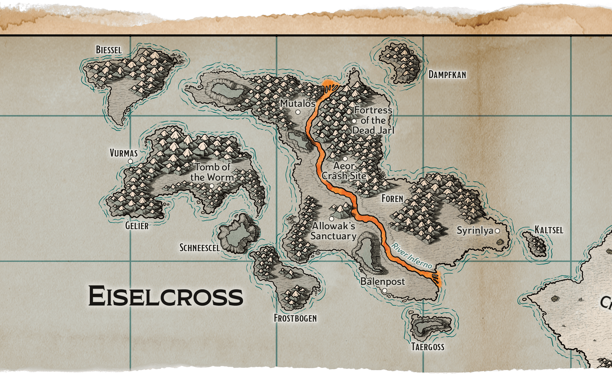
Part of the island group known as Eiselcross is to the North and West on the above map (with Syrinlya at the Southwest end), and here is a link to the map of the Eiselcross area itself.
https://media.dndbeyond.com/compendium-images/egtw/yDOyqyOocErRgYJK/3.7-Eiselcross.png
Palebank Village
Our hardy pre-heroes met up in the little hamlet of Palebank, on the continent of Wildemount. They found that Palebank is quite small, certainly no shops dedicated to magic or magical weapons, though there is a store that sells general goods and maybe a potion or two which they have yet to visit. Three of the party’s elves, Budgerigar, Kirknarnan and Feanor had acquaintance with each other owing to their lineage. Connections with the others in the party, Gandoff, Delenn and Popeye were less certain. Some may have journeyed by ship to reach Palebank, others may have come overland.
The Graveyard
Seeing that the town was nearly deserted, the found out that there was a funeral that day for a Dwarf, Urgon Wenth. While they were paying their respects, they were approached by Elro Aldataur an elven resident of the village who seemed to posses some authority and respect in the town (he is in fact the leader of the Village).
They learned that Urgon had visited the island area to the Northwest of Palebank called Eiselcross for about a year, in search of adventure and treasure. Urgon had returned two months ago, after exploring Eiselcross. A few days after his return, he started moving quite slowly and blue veins appeared on his body. The priests of the nearby villages tried with various spells to heal Urgon, but nothing worked. Eventually his body turned to ice, and so he died.
Elro also revealed that a second Dwarf had become ill, Tulgi Lutan, who seemed to be moving more slowly than normal, with a distinct blue color to her veins, and he explained that when he approached Tulgi to try and obtain more background information on the affliction, she rebuffed him, having no trust in authority, and asked that she be allowed to die in peace. Elro suggested that they visit Urgon’s cabin near the edge of town and/or Tulgi’s Cabin, nearby, and that he would make sure that the party was authorized to have access to Urgon’s cabin.
Elro offered 100 gold pieces for uncovering the cause of the affliction.
Urgon’s Cabin
With plenty of time left in the day, the adventurers decided to take Elro up on his offer, and trudged off in the snow. There they found a guard named Mila Teno, one of the “Glassblades”, who seemed to already know of their approach and agreement with Elro. The group entered the cabin, and began an investigation. Things were strewn all over the floor the cabin, as though it had been robbed or someone had been there looking for something. While taking a close look at the books, a bookmark was discovered which turned out to be a receipt for the sale of certain items by Urgon to Pelc’s Curosities, an antique shop in town. The items were listed as a dagger, a scroll case, a jade statuette, a quiver of twenty arrows, a silver ring set with a jasper, and two blue glass vials. Examination of the cabin and the surrounding grounds also led the adventurers discover some tracks in the snow which appeared to lead to Tulgi Lutan’s Cabin.
The group were concerned with what they eventually figured out was the head of a Yeti, mounted above the mantle, and wondered if perhaps it could be a factor in the mystery, as they are native to Eiselcross.
Tulgi’s Cabin
The group arrived at Tulgi’s cabin, only to find the door locked. Despite thie locked door, there were clear indications of someone within – smoke from the chimney and the light from a fire peaking through the shuttered windows. When Kirknarnan knocked, Tulgi made it very clear that she wanted everyone to leave her alone, but though a combination of charm and good luck, Kirknarnan and the rest of the group were able to gain entry to the cabin.
They found the cabin to be extremely hot. Indeed Gandoff only barely missed setting his robes on fire from standing too close to the hot brazier. Through some “persuasion” with the force to back it up, the group convinced Tulgi to divulge what she knew. It wasn’t all that hard, as she figures she is “dead meat” anyway.
Tulgi came to Palebank Village a few years back from Shadycreek Run with her sister, Hulil. Both work for the Uttolot family. The Uttolots sent the sisters and a few others to the village to keep an eye out for treasures coming back from Eiselcross—with the intent of stealing them. When such artifacts come through the small settlement, they are often unusual goods that treasure hunters are trying to keep away from Uthodurn or the Dwendalian Empire, the major ruling force on the continent. When Urgon Wenth returned to Palebank Village with treasures from Eiselcross, Tulgi saw her chance. She waited for Urgon to sell his finds to Pelc’s Curiosities, then stole them all.
Tulgi gave most of Urgon’s relics to her sister, Hulil, but kept one for herself—an ornate dagger, which after a couple of tries the group discovered. Tulgi offered the dagger to the group, but the group declined, fearing it could have a part to play in the affliction. Delenn cast a spell to determine if the blade was evil or not, and reported that she did not detect any evil. Tulgi admitted that she was the one who searched Urgon’s cabin, convinced that the dead dwarf must have had magic or other secrets stored away there.
Tulgi also told them that Hulil has the other items in a site north of the village known as Croaker Cave. The group discussed whether to go to Pelc’s Curiosities or Croaker’s Cave, but owing to the diminishing light on a short Winter’s day, opted for Pelc’s Curiosities.
Pelc’s Curiosities
When the adventurers arrived at the store, they found the door ajar. After a perhaps ill-advised immediate entry, they discovered a band of bandits there and battle ensued. Our developing group quickly subdued the villains, with Budgerigar and Feanor playing pivotal rolls, terminating the lives of three bandits, and tying up the remaining two.
Upon questioning one of the remaining bandits had little choice but to “fess up” or die. The bandit revealed that they were in the employ of Hulil Lutan, Tulgi’s sister, who holds forth at Croaker’s cave, and that Hulil is also sick, moving slowly with blue veins on her body. Hulil had ordered the bandits to rummage through Pelc’s Curiosities in search of potions, scrolls, or other items that might help cure her. Despite their thorough search, the bandits found nothing useful.
The bandits also revealed that Hulil is a dwarf priestess of Tiamat, the “Scaled Tyrant”. Tiamat is the evil queen of dragons – a goddess of greed, envy and hoarded wealth, and patron of most chromatic dragons.
When Popeye ventured into the back room he discovered the owner of the shop, Verla Pelc, frozen like what modern day people in our plane of existence might call a Popsicle.
Having defeated the bandits they found them carrying no “coin” but did “relieve” them of their weaponry, perhaps to be pawned later for coin. At this point, the adventurers, weary from their battle and investigations, decided to seek respite for the day at the local Inn.
During the day, Kirknarnan was discovered to have an alter-ego “Tough Bandit” attached to his representation on the gaming plane. The all-powerful DM cast a spell the next day to banish the corrupted container to another folder of existence, renaming him “Kirknarnan the Broken” and the former adventurer bequeathed all that he was and all the he possessed to the reconstituted Kirknarnan, who seems none the worse for wear.
[DM Ed: I decided to leave it there, rather than moving the characters to the Inn. We can do that next session, and thus everyone can learn how to apply a Long Rest to their character.]
A Visit with Elro
After dispatching with the thieves occupying Pelc’s Curiosities, the group did a little exploring to see if there was more to be seen in the shop building, but came up empty. There was some consternation about the two thieves who remained alive: some in the part were not comfortable just leaving them be, and others were concerned that they would likely trot back to Hulil’s hideout at Croaker Cave, only to be fought yet again. So, they left Budgerigar Tealeaf to guard them, went to town in search of Elro to report on their progress.
Elro sent Mila over to the curiosity shop to relieve “Budgie” who returned a short time later. He was saddened to hear of the new that Vela Pelc had become a frozen icicle, and not terribly surprised to learn that Hulil Lutan had also fallen ill. Elro provided the adventurer’s with directions to Croaker cave, which the village generally knew was the abode of giant frogs and toads and thieves as well.
The group, slowly becoming friends over their shared experience spent the night at the local Inn and awoke the next morning with wounds healing and spells refereshed.
After breaking their fast, a quick visit to the local general store in town provided some much needed gold in exchange for the weapons recovered from Hulil’s band of thieves the day before. Soon they were off to find Croaker Cave.
Croaker Cave
The cave area was not difficult to find. There was only one obvious entrance, and a fair amount of exploration by “Cap’n” Kirknarnan revealed no alternate entrances. Near the entrance, a bit to the east, they could see smoke rising out of a fissure in the rocks above the cave area: it seems that the cave is occupied.
Near the cave entrance was a large pool of water. Careful investigation revealed a blue-skinned ice frog lurking just below the service. Approaching the pool, Feanor espied a heavy wooden beam. He also drew an attack from the giant ice frog, whose teeth were no match for even his meager armor.
Kirk attempted to wrap a ball of pitons on the end of a rope and cast the rope across the pool. That effort was successful, however there was nothing on the other side to hold the rope firm, and it was subsequently retrieved.
Battle ensued, and it soon became clear the there was more than one ice frog in the pool. Caught by surprise, its attempt to bite fell short. Concentrating on the first frog, Popeye and Budgerigar did sufficient damage that the frog exited the cave in an attempt to flee. However, in the escape attempt, it was finished off by a slash from Kirk, and perished.
That left the second ice frog known to be in the pool. Delenn then stepped up to the plate and from near the back of the group, cast a spell of Command on the second frog, and commanded it to flee. Although it took some damage in the process, it was able to escape the area.
Unfortunately, the ruckus attracted the attention of a pair of Hulil’s thieves. Based on their stature and build, it seems one of them is an elf, the other a dwarf.
Tune in next time for the next episode of “The MT Dungeon”, the Battle for Croaker Cave.
Croaker Cave – Continued
In Session #2 the group continued to explore Croaker Cave. The two aforementioned thieves started making guerilla attacks on the group from the other side of the pool while the group tried to figure out how they were going to get to the other side. After a spectacular failure climbing by Vash, a monk that Elros sent over to try and help, eventually Kirknarnan and Feanor managed to scramble up one side, while Popeye climbed up the other.
Vash did subsequently manage to climb up, but one of the thieves’ arrows found its mark, dashing her into the water, leaving her at the first stage of exhaustion. Once the group got across, they discovered that they had managed to disturb a host of annoying bats. Soon the bats’ numbers had been significantly diminished by attacks from the adventurers, and so fled the cave.
In doing battle with the thieves, the thieves managed to lure the explorers close to a second pool, where two more giant frogs awaited. These two were dispatched, along with two of what turned out to be three bandits. During the battle Delenn had ample opportunities to try out her wand of healing. Popeye managed to grapple the remaining thief who seemed pretty scared and unhappy, and revealed that Hulil Lutan is residing further into the cave, but plans to set out for Shadycreek Run, hoping that trading some of the items her sister Tulgi stole from Pelc’s Curiosities will allow her to pay for healing that will cure her. Poor dwarf: she does not yet seem to know that that sort of cure had already been tried, and was not helpful.
The hearty adventurers were considering whether to bed down for the night and rest when the session ended.
Hulil Lutan’s Hideout in Croaker Cave
Picking up in session #3, the group decided against a rest period, perhaps being unsure if there were any more bandits about. Exploring the cave Budgerigar, Popeye, Gandoff and Vash started rummaging through the bandit campsite. The fire was cold, and so was the pit that Budgie managed to fall into. A rope, with a lift from Vash and then the very strong Popeye quickly got her back above ground. Continue to examine the bedrolls, Budgie also managed to uncover a bottle of Bad Dwarf Whiskey, which is said to be quite a bit more sought-after than the what used to be in the bottles of swill that littered the floor.
Kirk, Delenn and others traveled up the passage to the North of the encampment, but they quickly discovered this just led them back to the bat cave (and not the one Robin frequents). The group then proceeded up the other passage, to the Northeast, and discovered another pool. Perhaps through luck or perhaps a shrewd guess based on the giant frogs in the other pool, Feanor discovered that there was indeed an occupant in this third pool – not just any old frog, the the giant toad Old Croker himself. He also managed, through exceptional animal handling, to convince Old Croaker to ferry him across the pool – and the rest of the party as well, though Popeye opted to use his above average strength and athletics ability to scale the wall and get to the other side on his own. Meanwhile Gandoff went back to see if he might retrieve the plank that most of the party used to cross the first pool, only to realize it was far too long to be able to make the necessary turns to get to the third pool.
For a while the group managed to quietly assembly on the far side of the third pool. They espied a large dragon mural on the North wall – likely a rendition of the evil dragon Tiamat. There was also a roaring fire in the middle of the room. Eventually their discussions alerted Hulil and her companion in worship of Tiamat to their presence. Hulil was annoyed by the presence of the party on what she considered sacred ground dedicated to Tiamat. Tense moments ensued and a brief battle erupted, as Hulil was skeptical of a couple of group members’ claims that they were there to help. In the process, Vash got a little too close to the roaring fire for comfort and got singed, and Budgerigar got hit with a sleep spell casted by Gandoff . Eventually Hulil was convinced by Budgie that the group really was just trying help.
Along the way, one of the group also discovered that the stone chest in the middle room appeared to be trapped with a strange blue powder in some small holes in the chest, which also is emblazoned with the image of a dragon.
When finally convinced by Budgereigar that perhaps the group was trying to help, Hulil Lutan demanded that her companion be awakened before she would discuss anything further. After that had occurred, Hulil revealed several bits of important information:
- The disease from which Hulil Lutan and her sister suffer from is known as “Frigid Woe”
- Hulil believes that she contracted the ailment from one of the blue vials that Tulgi and her bandits stole from Pelc’s Curiosities. That particular vial was cracked when she and Tulgi handled it, revealing that the vials’ lovely color was the result of a dark blue dust clinging to the interior surface of the vial.
- She plans to go to Shadycreek Run before the malady runs it’s course, hopeing to trade the goods that were stolen in exchange for a cure.
- Hulil sold one of the vials to a human named Irven Liel, a merchant who was traveling with his family, and was staying at the Jolly Dwarf Inn in Palebank.
Hulil was adamant that she would not reveal nor provide the contents of the chest to the explorers – who, after all, had claimed they were there to help.
Our fledgling adventurers then discussed at length what to do next. Things took an unexpected turn when Gandoff, for reasons known only to himself, decided to attack Hulil’s companion with magic missiles, leaving her nearly unconscious, lying on the floor of the cave. This naturally enraged Hulil, and as the session ended, it seemed likely that another battle would ensue.
Advice from the DM: Several of the characters (Budgerigar is a notable exception) seem to not be played in their alignment, and/or perhaps some of the players don’t fully understand what the characteristics of their character’s alignment might be. Below is some “homework” for reading up on alignment and how it affects characters’ behavior. Feel free to engage in discussion on this topic on the MT Dungeon Facebook group page, too.
A simplified explanation from the D&D5e System Reference Document (SRD) can be found at https://dnd5e.info/beyond-1st-level/alignment/
A discussion of alignment that goes beyond the basic rules can be found at easydamus.com – perhaps starting with easydamus.com/neutralgood.html
In particular, the DM notes for the benefit of the players that it is not absolutely necessary for evil beings to attack good beings, or vice versa – motivations are more complex than that, though I do recall one particular Paladin back in the day who was sworn to do so, and occasionally had to be restrained from leading the party into disaster.
Hulil’s Hideout — Continued
As session #4 got underway, the group decided to try and heal Hulil of Frigid Woe. Out of healing spells and as Kirk had gone to the shore of the pool to find a way back, it fell to Delenn to use her Wand of Healing. While this had no effect whatsoever on the mysterious illness, it did manage to gain some good will, which dispelled the potential for additional combat.
The group again debated what to do with the stone chest: whether to try and open it, carry it out (apparently not noticing/remembering that it was large and heavy and made of stone 8)) and what to do about the occupants of Hulil’s hideout.
Hulil Lutan made it quite clear that she had no intention of opening the chest, sharing its contents, or doing anything else for the party so long as her companion remained seriously injured but did promise to share any additional information she might have about the disease if her companion’s health was restored. Having first healed Kirk, DeLenn again used her want to heal Hulil’s companion, Raegrin Mau, who had been heavily damaged from Gandoff’s attack, moaning in pain on the floor. It unsurprisingly turned out that Hulil had indeed shared all the information she knew during earlier discussions.
After some debate, considering whether to spend the night in the cave or return to town, the troupe decided to depart. Her companion restored, Hulil was more than happy to call up Old Croaker to get the riotous adventurers out of her hair. On the way out of the cave they came across the tied up bandit from earlier in the day, and carried him with them.
When they got to the pool near the entrance way, the plank they found earlier was extended across the pool and most of the party crossed without incident, leaving Popeye and the tied-up bandit on the far side of the pool. Clearly the plank was not going to hold up under the weight of Popeye and the bandit, so after some discussion they had Popeye untie the bandit’s feet. The bandit immediately got up and started running away, since nobody was holding on to him with a rope. Popeye gave chase, but soon the bandit had reached Old Croaker, and being a known comrade quickly negotiated his transport across the pool and disappeared from sight.
The Jolly Dwarf Inn
Our hearty adventurers looked for the village leader, Elro, but he had apparently returned home for the night. Needing food and rest, the group sought the local inn for a meal and much-needed sleep.
Having inquired with the bartender, they discovered Irven Liel, Fenton and their daughters, Magic and Honor at a table having dinner — Irven was known to have recently purchased a blue vial from Hulil. During a pleasant discussion with the family, the family learned that the blue powder in the cracked vial, now wrapped in cloth, that they had purchased from Lulil was dangerous, causing the death of Urgon Wenth and Verla Pelc, and serious, debilitating illness it the dwarven sisters Hulil and Tulgi Lutan. Upon hearing that they were very frightened, and proffered the vial, still wrapped in cloth to the party.
The next morning, after they had broken their fast, they were greeted by Elro Aldataur, who thanked them for the information they had, and promised to make good on his offer of 100GP for solid information on the origins of the strange affliction. Elro departed, the artifact in hand, to conduct research to see what might be learned about this strange and dangerous blue powder, but before he left requested that the crew stay in town until he could investigate.
After a visit to Tulgi Lutan to deliver the news concerning her sister, Budgerigar went to the village general store in search of holy water. The shopkeeper there indicated while they didn’t have any stock at present, that they do have it from time to time.
Kirknarnen went in search of weapons. The store only had the most common of weapons, which the party already possess. The village has a blacksmith, but only a small forge suitable for small parts — hinges, clasps, rings, nails and the like – nothing big enough or hot enough for forging weapons.
Point of information: contrary to what I had believed, sailing ships (consistent with the general technology in Wildemount at the time of the adventure) did sometimes have tiny forges for making very small metal parts for the rigging, and most often were with the sails stowed, and not used underway (though maybe in calm waters.) Here is an example:
https://sites.scran.ac.uk/voyage_of_the_scotia/scotia/vs031-060.htm
Frigid Woe
A day later Elro returned with news. Firstly, Irven Liel and family have also contracted Frigid Woe. Secondly his check into history reveals that the only known cure for Frigid Woe is a milky liquid the Aeorians stored in gold vials. The only real hope of finding any would be in the area around Eiselcross, where Urgon Wenth had been exploring. Elro offered 200 GP for the task – and of course reminded the group that time is of the essence.
He was also heartened to learn that the group had not attempted to open the stone chest. It is clear to him that the blue powder in the chest was most certainly the same substance placed there as a trap, and that depending upon how the trap worked, even the simple act of touching the trapped chest might have proven calamitous.
He said that he learned that the disease is such that it generally takes about 2 months for the effects to become fatal. Still that isn’t much time, especially for Tulgi, who came down with the malady about a month ago, and requested that if the adventurers wish to undertake this task (which the DM heartily recommends, unless they want to wait a month for new content to be created ;)) that the heroes meet him at the docks the morning after tomorrow.
Elro also warned that Eiselcross, being part of the frozen North is very sparsely populated, and COLD, and suggests visiting the store to purchase or rent the very warmest winter clothing that can be found there.
I finally did find a nice map of the Wildemount world online. (See the beginning of this page).
Session #5: Off to Syrinlya on the island of Foren in the Eiselcross group.
Our adventurers found themselves feeling “buff” – after leveling up to level 2. This required that they make a number of choices, along with acquiring new skills and for some, spells (and for some of those their very first spells).
It was then off to the shop to purchase essentials (notably extremely warm clothing) and sundry for the trip and adventure on Eiselcross. Budgerigar paid one last visit to Tulgi Lutan in her hut, and in so doing managed to extract some coin to offset some of the costs of undertaking the adventure to find a cure for Frigid Woe.
Our tired shoppers then took their repose for the evening, and awoke the next morning to travel to the docks for their passage on the Remorhaz, a ship that acts almost like a ferry, transporting adventurers between the mainland of Wildemount and the islands of Eiselcross. The voyage was uneventful, with only a couple of days severe enough to make our heroes seasick.
Arriving in Eiselcross, the group was first struck by how very cold it was there. The outpost of Syrinlya consists of a few fur lined yurts. They were greeted at the docks by one Morgo Delwur, who quipped “Don’t worry! It’ll cool down here eventually”. It seemed that there might be more to her than met the eye. Morgo was happy to guide them around and describe who lived in various yurts. From Morgo they also learned that a lot of adventurers come through looking for treasure at the Aeorian crash site.
One stop was at “The Buyer’s” hut. The group had been told to seek out The Buyer once they had a cure for Frigid Woe. Figuring that this person might be important they paid him, and his green faerie dragon an uneventful visit – though the hut itself was interesting, with runes on the walls. They learned there that The Buyer can teleport items between two stone chests – perhaps similar to Vanishing Cabinets used by witches and wizards here on Earth.
Another stop was at the yurt of Orvo Mustave. Orvo was saddened to hear the news about Urgon, as they often traveled together. Orvo told them that the found the blue vials in Salsvault, an Aeorian ruin partially submerged in water in a region of Foren (the largest island of Eiselcross) where the glacial ice is thin, called the “Thin Sheets”. It is located about 200 miles north of Syrinlya, somewhat near the River Inferno.
The River Inferno is a mile-wide river of lava, springing up seemingly from nowhere. Most scholars believe that the drive was created by the crash of Aeor, though this theory has not been confirmed. Oddly, while generally the river is disastrously hot, as one might expect, ice and snow that fall into the lava remain intact. Bold explorers have been known to ride floating icebergs on the river Northward at an impressive rate of 7 miles per hour. Fire elementals, magma mephits and salamanders can occasionally be found along its banks.
Inquiring further, our adventurers learned that while pieces of Aeor were thrown all over Eiselcross and the surrounding Frigid Depths. The crash originally caused a three-mile diameter crater, as though the city had fallen from the sky. Ice has now covered most of the crater, but ruins do poke through to the surface, creating tunnels, pits and chasms. The ruins are filled with dangerous, wonderful creations and pockets of people frozen in time, and all attempts to break or dispel or otherwise remove the impenetrable magic barriers have failed.
Orvo and Urgon found the ruin by following an Ice Mephit, as the creatures seem to be drawn to the magic of something there. Orvo thought that the ruin might be as well preserved as it is because the structure was reinforced with magic. It seems to have been some kind of laboratory or other – but they didn’t stay long – they only got into three chambers before being chased away by animated suits of armor!
The group tried to convince Orvo to accompany them, but were unsuccessful. Orvo mentioned that a large party was gathering to search for possible survivors of an expedition led by Professor Gulrim Shalebrow, which itself went to search for the origin of the strange magic in the region of Mutalos, but never returned.
Orvo immediately sold his share of the treasure to The Buyer, whereas Urgon took his back to Palebank Village.
When asked about a place to camp, Orvo suggested using Bertron’s Yurt. Bertron was, as Orvo put it, “a rich fool of an elf who came looking for adventure, but found the inside of a saber-toothed tiger instead”. In Bertron’s yurt they found additional rations and other useful bits of kit, which were shared among the party.
Session #6 – The Trek to the Aeorian Crash Site Begins
After an unsuccessful brief search for a sled that they might use on the way to their next destination our hearty adventurers headed SSW and then NNW on their way to the Aeroian crash site near the middle of the island of Foren, the largest of the Eiselcross group – a trek said to be around 200 miles. During the first day’s journey, Kirknarnan located some saplings suitable for a frame for a sled, cut them down, and dragged them along the way.
After the evening repast, Kirk sat down to invoke his Goodberry spell, with seven of the magical berries appearing in his hand as a result. During the watches during the night, the appointed sentries overheard some thrashing noises maybe 50 to 100 yards away. Nothing could be located at night, but the next morning some odd tracks were discovered: some were kind of “Y” shaped, and the others seemed akin to very large mammalian paws. Curiously, these tracks lay together – not side by side, but almost as though a single creature had made them. No other trace was found, however.
Near the end of the the second day of travel, the treacherous ice sheets were encountered. As they moved carefully forward, they espied some figures maybe a mile ahead – it was hard to tell exactly how many. A bit of observation revealed that these folk were headed in a somewhat more northerly direction as opposed to parallel to the River Inferno, know to be to the West, so the group headed towards the unknown travelers. Shortly thereafter, some tracks were located, clearly two sets of boot prints side by side, traveling about the same speed as our adventurers.
As darkness fell, the evening meal was taken of the goodberries prepared by Kirknarnan the evening before, and then he and Budgerigar followed the tracks as best they could in order to investigate what the other travelers might be about. They soon came upon what seemed to be a quickly constructed lean-to shelter near a small group of trees. Rather than disturb them, they chose instead to return to their own camp and informed the group of what they found. Kirk once again employed his Goodberry spell, with five berries appearing as a result.
The next morning the troupe arose early and followed the tracks that Kirk and Budgie had followed the previous evening. Discerning that the occupants were just arising, a couple of the team hailed the unknown travelers, and two “wildfolk” scouts appeared out of the shelter.
The scouts spoke Common language and a parley ensued. While wary of the much larger group that had followed them, the scouts were not unwilling to share what they knew, particularly after our heroes offered them some arrows to replenish their supply which had been completely spent hunting a saber-toothed tiger – tracks from which our travelers had perhaps seen between their own camp and this one.
The scouts seemed to be simple folk, and were “sore afraid” when mention was made of the Aeorian crash site – evil things were said to happen there. The only concrete advice our team obtained from the scouts was to travel with rope attachment, as falls through the thin ice sheets were said to be somewhat the norm. Learning that the scouts were headed in a more northerly direction than that which leads to the crash site, the two parties went their separate ways. Mention of the tracks of what seemed like a very large bird and a very large mammal didn’t make them any more comfortable, and when the party described Ice Mephits to them, their response was akin to Gollum’s when Sam Gamgee described “oliphaunts” – they didn’t want such creatures “to be”.
The third day’s journey was otherwise uneventful, and camp was made on the ice as the sun set. Kirk shared his more limited supply of goodberries, while Vash and Gandoff consumed a normal day’s rations instead. Kirknarnan once again cast his Goodberry spell, and once again five berries appeared, for use the following day.
On the fourth day out, the probable happened: one of the travelers, Kirknarnan, fell through the ice. Retrieval was uneventful, and aside from being soaked up to his chest, and being a bit tired, Kirk was none the worse for wear – nothing that a good night’s rest and a warm fire couldn’t cure. There we left our adventurous traveler’s, bedding down for their third night on the “Thin Sheets”, a bit more than 100 miles under their boots.
Session #7 – At the Doorstep
The next day the adventurers continued on their way to Salsvault. About 20 miles from their previous camp, they encountered a mage from the Cerberus Assembly, named Wayne John. Wayne was very cold, but a could of Kirknarnan’s goodberries created the previous night helped. Wayne explained that he had been accompanying some dwarves to Salsvault, where the dwarves had all perished. He explained that he was “cousin” to one Pumat Sol (but of a different race than he), another mage of the Cerberus Assembly who runs a magic shop in Zadash.
(See https://www.youtube.com/watch?v=dGv-_8tk8g4 about 3:10:30 into the video for something truly entertaining.)
The next morning as they began to prepare food for the morning Wayne John vanished on the spot. However, noticing that there were no tracks leaving the spot, the group correctly deduced that Wayne was still present. As he tried to move, the group noticed the rustle, and called out that they meant Wayne no harm, and he reappeared.
Kirknarnan suggested that Wayne could accompany them back to Salsvault. Discussion of the groups membership ensued, as Wayne was not initially thrilled with the idea of returning back to a place where he has watched another party killed off, but in the end he agreed to come along, with the terms being that he would be allowed to retain the first Aeorian artifact they found, aside from cures for Frigid Woe.
Our explorers then broke camp and continued on their way to Salsvault. At that point something unexpected happened (unexpected even to the GM), and they it seems they had teleported 60 miles closer to Salsvault. (Oopsie).
As luck would have it, they very soon discovered some Ice Mephit tracks and followed it to the vicinity of Salsvault, where the more perceptive members espied a couple of Ice Mephits near the door. Also discovering that the door was frozen shut, the decision was made to spend the night about a mile from the entrance.
The next morning, attempts were made to open the door. Torches proved more or less ineffective. Fire-based spells and whaling away at the ice with picks and crow bars worked better. Finally, Budgerigar managed to free the door from the remaining ice with brute force.
During this process some attempts were made to communicate with the Ice Mephits, who didn’t seem to be interested in talking (or perhaps did not understand what was said.). But when one adventurer tried to communicate with them in “infernal” their attention was drawn to the group, and battle was enjoined. After taking some hits, the Ice Mephits were eventually dispatched.
The door was opened, and the party discovered that the door was guarded by 3 animated suits of armor, which was not entirely unexpected as both Orvo Mustave and Wayne had indicated such denizens occupied the structure, along with reports of zombies and flying sharp-edged weapons. And that is where we left our group, at about 11AM on that game day.
Session #8 – Danger Will Robinson!
The group picked up where the left off, and after considerable discussion decided to see if they might sneak past the animated suits of armor. Delenn once again used her staff to assuage the wounds inflicted by the ice mephits earlier in the day, and Kirk provided one goodberry each to Budgie and Vash. Unsurprisingly, any hopes that the armor might not attack were quickly dashed, though Kirk did manage to get past them without being immediately attacked in the process. A pitched battle then ensued, as the armor was, well, well armored.
Everyone in the group contributed their various skills to the encounter, with Budgerigar, Kirknarnan, Feanor and Popeye being the most bloodied from participation in melee with the armor.
In the process Budgerigar was rendered unconscious, and took one step towards the river Styx. However, near the end of the battle life returned to her body, though not with much vigor. The battle ended, our adventurers decided it best to remain in the first room for the rest of the day and night in order to lick their wounds. Kirk also decided to create another batch of goodberries, though as bad luck would have it, only two appeared this time, just like last time.
Given a little time, Delenn and Vash were able to make out the inscription on the East wall, which read, in a variation of Draconic
Welcome to Salsvault!
Visitors, please wait here for an escort and
DO NOT TOUCH ANYTHING WITHOUT PERMISSION.
During the night’s watches, there were some thumping/banging noises heard with some regularity, and on the final watch of the night considerable banging was heard through the wall to the East (below them on the map), but no encounters demanding their attention occurred. As luck would have it, Delenn’s wand “awoke” completely refreshed as well, leaving the group ready to proceed onward into Salsvault.
Session #9 – Into the Vault
After a good night’s rest, disturbed by the aforementioned noises that even shook the wall to the East, our troop awoke refreshed and ready to tackle a new day’s adventures.
Investigating the first room the South refreshed Kirknarnan’s memory of seeing Dwarven footprints there, and Wayne John indicated that the Dwarves he accompanied didn’t even get past the animated guards. Moving on to the South they discovered a room that had footprints leading off to the North and back again — perhaps those of the animated guards they had fought the previous session?
Then carefully opening the door to the hallway to the East they observed some shuffling figures in tattered robes – perhaps these were the origins of the less violent noises the evening before. Deciding to take on whatever was there, they opened the door fully, and battle commenced. The battle was rather uneventful except that Budgerigar did take a couple of hits on the nose, upon which she retired until the battle had completed. Delenn obliged with a couple of uses of her staff of healing – which once again fully recharged with the night’s rest later.
They also noticed a door marked with a rather large red “X” – to the room which had been located to their East, and from which loud noises and crashes could still be heard.
Proceeding down the hallway to the East, a couple of adventurers listed at the door to the South, detecting some bubbling sounds. Winds could also be heard at the doorway to the North – as though that were outside. At first hesitant to enter the Eastern doorway, it seemed like their best option to proceed. Upon opening the door, they were greeted by a rather white figure with red eyes, Ferol Sal, who immediately demanded why out adventurers were in Salsvault, and interfering with his work to find a way to punish the gods for causing Salsvault to crash into a completely different continent from its origins.
Resorting to the truth (what a concept!), they convinced Ferol that indeed they meant no harm and were mostly looking for a cure to Frigid Woe (which, it turns out, was the results of one of his experiments). He indicated that the cure could be found in the room across the hallway in a chest -which was locked, but that he had the key. He shrewdly suggested they bring the chest back and he would open it (knowing full well that such would not be possible), and attempts to persuade him to provide a key by offering help in his work were not very successful, as looking at the rag-tag group quickly convinced him that they were not very likely to be of any help.
Rebuffed by Ferol Sal, the group left and opened the door to the North. There they were greeted by wind and waves – the submerged East side of Salsvault (I guess one could call it the Lower East Side. 😉 ). With their superior perception, two of the group (at least) quickly noticed some giant crabs lurking below the surface, and a chest – made of stone – submerged along what had been the Eastern wall of Salsvault.
The crabs proved tough to eliminate. Somehow the arrows seemed to skip off the water, were deflected by their tough exoskeletons, or missed their mark completely. Finally Delenn managed to hit one with some sacred flame. Others found more success with darts, and eventually even arrows seemed to sink in, and the crabs were vanquished – and one was used to make a tasty meal for the campers later, as they occupied the entrance room for a rest once again.
The chest proved harder to tackle, and only Popeye was able to make a dent in the stone cover. It was tough going – the water was cold. Thieves tools were hard to use under the water, and the cold water took its toll on the physiques of Kirk, Vash, Feanor and Popeye – with Kirk being particularly worn out. Unfortunately, a goodberry or two did nothing to help the situation.
Getting ready for the next day’s exploration, Kirknarnan once again cast his Goodberry spell, and four berries subsequently appeared.
Session #10 – The Cure, Rug and Robes
Having rested and fully recovered from the previous day’s attempts at opening the chest, the troop headed over to the room with the chest for another kick and the can, as it were. Luckily for them, no new giant crabs showed up looking for revenge for their mates’ demise.
This time luck was with the group, and the lock on the chest was picked successfully on the second try. Once opened the chest revealed 20 vials with a golden liquid, presumed to be the droids cures they had been looking for. Feanor and Vash retrieved them 6 per trip into the water, Feanor getting a little too cold in the process. In order to evade a possible future catastrophe, the vials were split up, four per person (excluding Popeye whose character traits might put the vials at risk, and Wayne John who was not there for the cure anyway.) The chest also included a strange looking artificial eye
Returning back to the entrance room, Feanor asked if Wayne might identify the eye. Doing so, Wayne indicated that it was “Ersatz Eye”, which could be used to replace an eye lost in battle or an accident, allowing its wearer to see through the orb somewhat like normal eyesight. Feanor asked if Wayne would accept that as the first treasure promised, to which Wayne agreed. However, Kirk suggested it be kept with the group, to be given to Wayne John later, which drew a somewhat sidelong glance towards him from Wayne.
Moving on, there was time to explore some more rooms. Shying away from the room with the red “X” identified by Ferol Sal as being a place it would be unwise to enter, after some discussion a decision was made to try the room across the hall to the South. Opening the door revealed a mess of broke and/or rusty knives, swords, daggers, spears and the like on the floor in disarray, but no other doors. Closing the door, Kirk asked for Wayne John’s professional assistance to determine if magic was involved in the room, and indeed magic was present. Kirk, with some trepidation, then opened it again and entered the doorway. He was immediately beset by a set of swords that were not being wielded by any visible hands – and nasty they were. Even withdrawing was perilous:
“In a fight, everyone is constantly watching for a chance to strike an enemy who is fleeing or passing by. Such a strike is called an opportunity attack.
You can make an opportunity attack when a hostile creature that you can see moves out of your reach. To make the opportunity attack you use your reaction to make one melee attack against the provoking creature. The attack occurs right before the creature leaves your reach.”
Near death, Kirknarnan was quickly revived by Delenn, consumed his four berries, and was then additionally nearly fully healed by Delenn. (Unfortunately Delenn’s prototype, Mira Furlan, lived in our real world, and passed away this past week at age 65, due to complications from the West Nile Virus.)
Once again eschewing the door to the North, our (birdlike?) adventurers decided to try their luck to the North. After a couple of tries, the lock in the door leading North out of the entrance hall was foiled, and they entered the room. There they found a couple of locked chests, a locked door to the West, an unlocked door to the East and a lever near the door to the West. The door had some draconic writing overhead, which Vash and Delenn soon translated as “Disease storage. Authorized Personnel ONLY”.
Investigating further, Gandoff and Vash spotted tiny letters with the word “Ice” on the two chests – both were rigged with traps, and the word itself seemed somehow connected with the trap. They also noticed that the lever had some weathered red paint. Checking for magic, Gandoff confirmed that the chests and the door to the West all had some magical aspect, (conjuration in nature) but not the lever.
Spending overnight in the entrance room, Kirknarnan once again cast his Goodberry spell using a spring of mistletoe, but this time, seemingly reverting to form, only two berries appeared. The watches were uneventful, aside from the now customary banging and crashing from the room to the East, and softer banging noises to the NNE.
The next day, with the cure seemingly in hand, the group proceeded to continue to explore Salsvault, perhaps in search of more valuable Aeorian artifacts. Once again proceeding North, they opened the door to the East, unsurprised by some zombies, once again in tattered Aeorian robes, that accounted for the noises from the NNE the night before. One of the zombies was separated from the group by a Thaumaturgy spell cast by Delenn, leaving two in the immediate vicinity left to fight. Feanor took the brunt of the damage, but between Feanor, Kirk, Popeye, Gandoff, Budgerigar and Delenn it was not long before the hallway was littered with zombie “pieces parts”. Feanor, hurt rather badly in the battle, was quickly healed to reasonable health by Delenn.
Gandoff, proceeding North on his own, was then surprised by the third zombie who lay in wait in a door to a room to the East, but the undead creature was quickly subdued. Investigating the room from which the zombie had emerged, four beds with trunks were found. Checking carefully, Kirk and Feanor were able to confirm that the chests did not seem to be trapped. Rifling through the chests, most contained just bits of old, useless clothing and knick-knacks, though Kirk did find one with an Aeorian robe, which he donned over his regular gear.
Taking on one more room, the next one to the North, a rather dark room was discovered – the magical light sconces illuminating most of the rooms and halls of Salsvault were broken there. Working through the pile of rubble uncovered two things: first, an additional Aeorian robe, and second, a piece of carpet or rug that seemed intent on suffocating one or more party members. To Ferol Sal’s dismay, as he learned later, this artifact was unsuccessful in grappling even one party member, and soon lay tattered and scorched on the floor. Budgerigar then donned this second Aeorian robe.
(There is a great episode of Critical Role, Campaign 2, episode 12, where a similar artifact has a much more “interesting” time. See https://www.youtube.com/watch?v=HoZGMqCIRK8&list=PL1tiwbzkOjQxD0jjAE7PsWoaCrs0EkBH2&index=12 – this encounter starts at about time index 2:40:00 the rug shows up about 2:43:00 and things get interesting at 2:48:00).
Robes and all, our adventurers then retreated for the afternoon to the familiar entrance room, seemingly to play cards and discuss their adventures of the day.
Session #11 – In the Octopus’s Garden
As the next session began, it was once again time to prepare for the night’s watch. Kirknarnan once again cast his Goodberry spell, but as seems to be the case lately, only a couple of berries appeared.
Budgerigar and Kirk in their robes, and the rest set off to explore the rest of the remains of the Aeorian crash site. After listening at a couple of doors, the troop decided to open the door to one particular room at the North end of the hall. They quickly discovered that it contained lots of kitchen utensils and what not littering the floor. With the previous bad experience with flying objects of a sharp nature, Kirk quickly pled that the door be closed and no more exploration of that particular room ensued.
They then turned to the room at the Northwest corner of the unsubmerged part of the building. The room was found to be immaculate, as though it had been tidied up over the years. Indeed, they later discovered that it was the bedroom of none other than Ferol Sal, whom they met earlier, used by both his original Aeorian form, and his reconstituted undead form. Ferol Sal also left a note there, in case his undead form should permanently perish, describing his attempt to find a disease strong enough for retribution against the gods themselves.
A chest was found in the room, and though close inspection by a couple of members discovered no traps of a mechanical or magical nature, opening the chest revealed a swarm of poisonous (and, as it turned out, un-dead) tiny little snakes. Fortunately the hearty adventurers were quickly able to dispatch the writhing little nasties, and discovered 1006 silver pieces, 45 electrum pieces (worth 1/2 a gold piece each), and 201 gold pieces in Ferol Sal’s stash, which were quickly pocketed. Divided 7 ways, that would be divided amongst the group, with the remainder portions going in priority order within the group (5sp, 3ep, 5gp).
After some curative restoration from Delenn’s staff, our hearty adventurers proceeded down the hall to the East. Listening at the room to the North the bumping and shuffling they associated with additional zombies were heard, and so it was decided to leave that room alone. Since no noises were emanating from the room to the South, entry was accomplished, and there Budgerigar noticed a very VERY large Octopus in the water, along with what seemed to be a case that might contain scrolls bobbing in the water.
With some luck, Feanor was able to get a crossbow arrow, to which he had attached some rope, to stick into the chest. However as the scroll case was pulled Feanor also stepped back through the door, and the arrow began to perceptibly loosen its grip on the case. The commotion also drew the attention of the octopus, seemingly none too pleased with the activities disturbing it in its lair. A fight then ensued, with the octopus finally attempting to retreat into its inky – but it was too late, and Feanor managed to loose a parting swing dispatching the octopus in the process.
It was then a fairly straightforward operation for Feanor to retrieve the scroll case, revealing two scrolls. Retreating to the main entrance they asked Wayne John if he might identify the contents of the scroll. He agreed, under the condition that if there was a scroll that he particularly valued, that he might be first in line for that scroll – with its value counted against his share of the overall treasure. Feanor was rather reluctant to agree to this, and the animated discussion that followed angered Wayne, who promptly disappeared, and suggested from the next room that the group reconsider, least he kill them all.
After a brief discussion, our explorers agreed and Wayne returned. Taking out a pearl worth at least 100gp, he pondered over the first scroll, identifying it as a spell scroll of detect magic. Repeating the process with the second scroll, using as second pearl, it too was found to be a spell scroll for detect magic. Wayne then turned the scrolls over to Gandoff for safe keeping.
There being time remaining in the day (although time is somewhat hard to track inside the confines of Salsvault), they decided to explore one more rom, close at hand, to the West. While the door was not found to be trapped in the usual sense, shuffling and bumping could be heard beyond it. Hopeful for additional booty of the material sort, entry was made. At first, the zombies only entered the doorway. Was it perhaps the Aeroian robes, similar to the tattered garb which they themselves wore which gave them pause?
Battle nonetheless ensued at the doorway where it was learned that these zombies had one additional trick up their tattered sleeves: it is particularly hard to kill these undead, since, when they seemingly had been dispatched back to the netherworld from which they came, they would nonetheless manage to cling on to their undead form. In the process Feanor was rendered unconscious, but Vash managed to drag him out of reach of the zombies and nigh to Delenn whose staff of healing quickly revived him, though he did remain someone disoriented for a short while.
Having had enough of zombies for one day, our now somewhat skittish adventurers retreated back to the main entrance room and settled in for what turned out to be an uneventful night’s watch. Kirk consumed his berries, which both healed him somewhat before the night’s watch, and also nourished him, removing the hunger resulting from the day’s activities. The rest partook of their regular rations for one day. Once again casting the Goodberry spell, Kirk had better luck, and six berries appeared this time.
Homeward Bound – Almost
(Disclaimer: The GM wasn’t in the best of alertness this night, and didn’t take careful enough notes, so some events may be out of order, or even missing altogether.)
After a night’s rest, the troupe decided to explore Salsvault just a little bit more. First up: more Zombies in room in the NE corner of the building (SE on the map). These were dispatched rather quickly, though Feanor required a dose of Delenn’s staff to be right and ready for the rest of the day. However, curiosity got the best of Vash, who attempted to pick the lock to the door. Failing that, she found herself moved in space (if not time) to another room, and was promptly attacked by animated cutlery. Fortunately, the quick thinking monk was able to make a dash for it, and get out the door just as Kirknarnen arrived to investigate (and to shut the door behind Vash). Indeed, it was the same room which Kirk had visited a few days back and also received a rather un-welcoming reception.
That was enough, and the group exited Salsvault to camp in the clearing where they had camped the night before entering the complex. Feanor sought to also bring along the rather heavy Aeorian armor (apparently no longer animated), and Kirknarnan built a sled to carry it. As weighed down as they were with their own clothing and supplies, that didn’t slow the party down much at all. Once camped, Kirknarnan once again cast his Goodberry spell, and, lo and behold, a full complement of 10 berries appeared in his hand, so no rations where required by anyone for that last day in Salsvault.
The next day the group started off fore Syrinya, and encountered nothing but cold, snow and the watchful eyes of birds and wildlife that day or that night. The next day and night were similarly uneventful. And so it generally continued, with all being quiet except maybe what sounded like the whimpering of a wounded animal, which turned out to be hard to track down and identify. The second evening out Kirk was again quite productive with the GoodBerry spell, and 10 more berries appeared, and all were refreshed. The following day, 6 more berries appeared as well. Thus three sprigs had been consumed thusfar, including the last night in Salsvault.
The fourth night out they heard some other noises, as though a hominid of some sort was traipsing through the snow, however a light spell cast by Gandoff was unable to (ahem) shed more light on the subject. This same night Kirknarnan went looking in a nearby copse for some sprigs of mistletoe, and as that is common in this frozen waste, managed to find 3 sprigs, replenishing his supply. After that, the adventurers were on their own, and consumed rations each day, simultaneously lightening their load.
The next day, the fifth day out from Salsvault, a strange almost zombie-like creature (one huge difference being that it was capable of speaking and understanding Common speech) crossed their paths, seemingly bent on revenge against a certain dwarf from Balenpost (where Wayne John was headed) – having been murdered by that very Dwarf. This vengeful entity seemed to have some kind of ethereal (or other) plane of existence connection with the instigator of its demise, and after some discussion, left him to go on his way, which was more or less perpendicular with their own path.
Aside from hearing what sounded like a wounded animal at night from time to time, not much happened until about 1 day out from Syrinlya. Firstly, Wayne John took his leave of the group, the “eye” in hand, paying a gold each to Feanor and Kirk for rations sufficient for the now easy journey ahead of him. Also on that day, they finally espied the source of the noise: a rather odd-looking creature with a bird’s upper body and a lion’s lower body with an arrow stuck in a wing: it couldn’t fly. As luck would have it, the Budgerigar and Gandoff were on top of the Animal Handling skills, and the creature allowed them to approach. However, when Feanor tried to do so, the creature began to be upset, and Feanor had to withdraw.
After Budgerigar tended its wounds, the creature seemed grateful, and bowed its head as an indication that it might allow her to ride, and indeed it was so. Thus the group re-entered Syrinlya, spending the night in Bertron’s, as before. The next morning they headed off to The Buyer, and arranged a deal whereby 18 of the doses would be magically transported to Palebank (10 for use in healing by Elro, and 8 remaining the property of the campaigners), and two doses retained by The Buyer, as payment for transferring the party’s doses as well as transporting the Aeorian armor to Palebank. (Elro and The Buyer have their own arrangements, which would pay for the transfer of the doses going to Elro.)
It turned out that the Aeorian armor was quite valuable for the simple reason that it is Aeorian – artifacts of that sort often bring in 5 times what normal equipment might fetch. The Buyer indicated it was likely worth around 9000 gp wholesale. The robes, being ordinary, were only worth 5gp – being Aeorian, 5 times what an ordinary robe might be worth, and it was decided that those who kept the robes would pay that price to the rest of the party’s members.
On the Road Again..
Having arranged to have the vials containing the cures for Frigid Woe and some rather heavy Aeorian plate armor magically transported to Palebank Village, the next morning the troupe once again boarded the SV Remorhaz bound for Palebank. The voyage being without incident, they once again found themselves at the Jolly Dwarf Inn. There they learned that the cure had reached all those in the area afflicted with Frigid Woe, though for Tulgi Lutan it was a very close call indeed.
Word having been sent to Elro Aldataur of their arrival, he arrived the next morning, payment in hand, along with pack animals carrying the aforementioned armor. From Elro they also learned that a new discovery of a somewhat dark manor, along with, surprisingly, a small village, near (but not too near!) the Ruins of Molaesmyr, on the other side of a fork in the Boreal Omen River, in the land of Savalirwood, about 250 miles to the South of Palebank Village, about half way to Shadycreek Run.
“Nearly three centuries ago, the forest suffered a terrible curse wrought from the disaster that felled Molaesmyr. In the centuries since, the fey magics have grown twisted and dark. Spirits and monsters crawl up from the cold, rotted forest floor, while shadowy whispers bring nightmares to those who sleep beneath the sinister trees. The forest has been renamed Savalirwood, for the elven word savalir, meaning “guilt”. “The ruins (of Molaesmyr) are considered the source the corrupt magics that still spread throughout Savalirwood”.
That morning they also renewed their acquaintance with Irven Liel and family, all of whom were beneficiaries of the cure for Frigid Woe. Indeed, they were sufficiently grateful to offer 90 gold pieces to the group to offset their considerable expenses and effort in acquiring the cure. Deciding that the adventure identified by Elro may be of interest, the group set about acquiring pack animals and gear to facilitate their trip South. They then also paid a visit to Tulgi Lutan’s hut, discovering that Hulil Lutan was also present. They managed to persuade Hulil to also provide some coin to cover their expenses (which drew a rather wry comment from Tulgi, still in bed, that she had also already provided some funding).
Having accomplished this, the group also felt a feeling of peace and energy flow throughout their bodies: time to level up!

