IBM 1410 FPGA: 1401 Mode “Zoned Out”

Having fixed the problem with the space, I continued to test out the IBM 1410 in 1401 mode. At first, I had thought that it was getting quite far in the diagnostic M011 – it would error out with the I register (instruction counter) at 6029. I spent the better part of a day chasing down an apparent problem with the Store A Address Register (SAR – opcode Q) instruction at the indicate location. However, when I placed a halt at the test before that, it still failed at the same place. How could that be?

So, I decided it would be worth the trouble to run the 1401 diagnostic in Instruction Fetch/Execute mode (I/E). The problem became apparent much more quickly than I had anticipated. After halting at the halt and branch instruction at location 2018, it ended up trying to fetch an instruction at a location near 06020. (My memory is just a little fuzzy on when that flying leap actually occurred, and I don’t have the output anymore.)

As you may know, the 1410 has 5 digit addresses, whereas the 1401 used 3 digit addresses plus zone bits to address up to 16K of memory. It was clear that somehow the translation from the 1401 style address to the 1410 address register had gone awry.

A little digging reminded me that there was one page of the automated logic diagrams (ALDs) associated with this translation, part of what is called the “Zone Adder” that was missing – page 14.18.04.1. After some time working with the xsim simulator under Vivado, I began to suspect a problem with my re-creation of the logic from that page.

  • Input “A”: -S ZONE ADDER A A DOT B A
  • Input “B”: +S ZONE ADDER B BITS EVEN
  • Output “O”: +S A NOT A DOT B A DOT B BITS EVEN

The output name is sufficiently complicated that the equation for this is not self-evident. Looking at the ILD figure 55, it looks like the following should be the equation:

O <= NOT A and NOT B — The NOT A is because A, above is -S not +S

Interestingly, page 14.18.04.1 is not referenced at all in the 1410 1401 Compatibility manual on page 7. On both the ILD and that manual, this signal is routed to the middle of a logical OR gate labeled “Zone Adder Carry”, which is laid out on page 14.18.06.1.

Regardless this VHDL caused the problem noted above. However, I had also penciled in on the ILD an additional inverter, which would be the signal without the added inverter (double negative and all that…). For that, the equation would be:

O <= NOT(NOT A and NOT B)

And it actually takes one less “fudged” gate, because the SDRTL provides this result outright.

It turns out that removing that inverter from the logic for that ALD (and thus implementing this second equation) cured that particular problem, both under xsim and running on the FPGA. But, at least superficially, this makes it look like it does not match the ILD — at least at first.

However, and finally, examining the page to which this signal is routed, 14.18.06.1, one sees that it is routed to a logical OR (physical NAND) gate where -S / -B active inputs generated the +S active output. So if one takes the two together, the end result is such that it does match the ILD.

The diagnostic didn’t get very much further, however, and now fails at location 2032 on a SAR instruction, similar to the failure after the “flying leap” problem, just at a different location. SAR is interesting in that it first copies the A Address Register to the B Address Register, and that is apparently failing.

IBM 1410 FPGA: “Space Cadet”

No, not that kind of cadet. Unlike the IBM 1620, the IBM 1410 does have adder circuits for doing addition (and multiplication and division as well). Instead, this issue had to do with the IBM 1415 space function.

I had thought that the principle instruction diagnostic, CU01, was working perfectly, but it was not quite so. I had noticed that even after finishing the diagnostic, I kept getting space characters sent to the PC support program, but figured that was just a software bug somewhere. However, when I started to run IBM 1410 1401 compatibility diagnostic M011, it stopped typing its instructional message to switch to 1401 mode on the console when it hit the first space character.

After some sleuthing, I discovered that the console typewriter logic never asked the channel for the character after the space – it just kept sending that space to the console typewriter again and again and again.

As one might expect, the issue turned out to be in the console typewriter Selectric emulation VHDL code. I had miss-interpreted the signal -V CON PRINTER SPACE NO to just involve console input via the space bar. a closer look at the related automated logic diagrams (ALDs) made me realize that in fact this was also the Selectric’s way of telling the 1411 that the space process had been completed, and that it really had nothing to do with input from the space bar.

At first I tried to just use the relevant states of the finite state machine (FSM) that controls spacing. That did not work right, however, because that same FSM also controls back-spacing. Qualifying the logic signal to only be active during a space, but not backspace, operation filled the bill.

IBM 1410 FPGA: Diagnostics!!!

With the console typewriter working, and the ability to load core images, I was now ready to try and run some diagnostics. The first issue I ran into was that the main diagnostics, CU01, was initialized for 80K of core. That the core image file was larger wasn’t an issue: the Windows based support program knows to only send the first 40K. However, there was a flag denoting machine size that needed to be “patched” — which I did using my emulator, and then saved as a new core image.

Loading the diagnostic, it typed out its identifier, but then quickly errored out with an Assembly Channel error on a Subtract instruction where the destination B-field was initially positive, but turned negative during the subtraction. This was not the first place I expected to see an issue – figured it would more likely relate to some trigger or other. But nope, this was a simple issue in the Assembly Channel.

The problem arose because the ALD diagrams I have are mostly for an IBM 1410 with the Accelerator special feature, however, most of the ALD diagrams for the Assembly channel proper (ALD 15.50.xx.1) are for the non-accelerated version whereas the Assembly channel controls (ALD 15.49.xx.1) are for the accelerated version. There were several signals that ended up either not being used, or having no source as a result:

  • -B B CH MIN+INV PLUS SIGN GATED
  • -B B CH PLU+IN MIN SIGN GATED
  • -B B MN +IN PL+PL+INV MN GATED

These all relate to cases where the B field ends up with a sign other than its original sign. I suspect that the idea was that these signals provided earlier gating to the assembly channel rather than just deriving them from the adder with additional gate delays.

After fixing the Subtract issues which involved just the “B” bit on page 15.50.06.1, (going from positive to negative) I immediately ran into the same issue on the first pass of the diagnostic during the same test, changing from negative to a positive result. Fixing this involved pages 15.50.05.1 (mostly). As a result the pages for the Assembly channel have some gates who’s note at the top is “FUDGED”. 😉

With that, so long as I didn’t enable I/O overlap and Priority Alert (interrupts) during the test, CU01 completed successfully! Frankly this was something of a surprise: It tests most of the instructions and ways of moving data and they all just worked.

Also, the run time of about 3.75 minutes matches very well with the information in the diagnostic listing for a 1410 with the Accelerated logic feature.

So then, I ran it again, but with overlapped I/O and priority features turned on in the diagnostic. It ran fine for about a minute, but then failed during overlapped execution of a multiply instruction. More on this during the next installment.

The FPGA Simulated IBM 1410 has a “pulse”

Having spent the past few months cleaning up my IBM 1410 SMS database program, and posting it to github at https://github.com/cube1us/IBM1410SMS , I have spent the past couple of weeks focused on the HDL (currently VHDL) generation, using GHDL and Xilinx’s Vivado toolset, with an eventual destination of my Digilent Nexys4 FPGA (Field Programmable Gate Array) board.

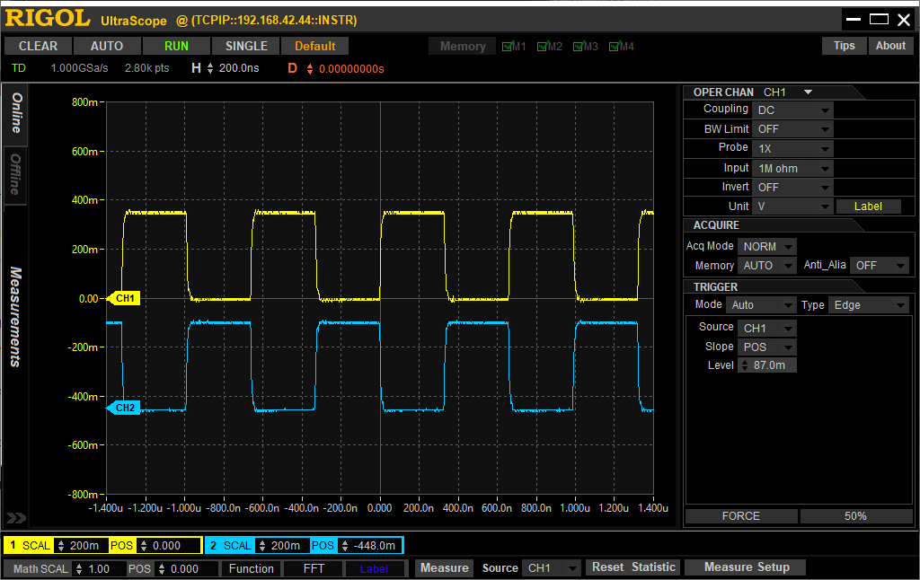
After fixing a few bugs, and implementing the oscillator (by way of a counter/divider from the 100 MHz FPGA clock), I loaded the results into the FPGA, and as show below, my IBM 1410 now has a clock, running at the right frequency for an IBM 1410 with the accerated throughput feature, as shown below:

IBM 1410 FPGA Clock
IBM 1410 FPGA Clock

On the original machine the lower signal, on channel 2 of the oscilloscope, was derived from the first using a delay line – about 330 ns of delay. Kinda hard to do with an FPGA. 😉 So, I implemented delay lines using a series of flip flops clocked by the 100 MHz FPGA clock – so, in this case, there are 33 of them.

This signal is not simulated – it is a real signal that exists in the FPGA.